2SK1764
2SK1764 is N-Channel MOSFET manufactured by Hitachi Semiconductor.
Features
- -
- - Low on-resistance High speed switching 4 V Gate drive device can be driven from 5 V source Suitable for switchingregulator, DC-DC converter
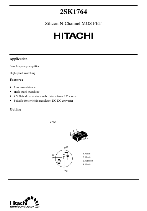
Outline
UPAK 2 1 4
D G 1. Gate 2. Drain 3. Source 4. Drain S
Absolute Maximum Ratings (Ta = 25°C)
Item Drain to source voltage Gate to source voltage Drain current Drain peak current Body to drain diode reverse drain current Channel power dissipation Channel temperature Storage temperature Symbol VDSS VGSS ID I D(pulse)- I DR Pch- Tch Tstg
2 1
Ratings 60 ±20 2 4 4 1 150
- 55 to +150
Unit V V A A A W °C °C
Notes 1. PW ≤ 100 µs, duty cycle ≤ 10 % 2. Value on the alumina ceramic board (12.5 x 20 x 0.7 mm) 3. Marking is "KY".
Electrical Characteristics (Ta = 25°C)
Item Drain to source breakdown voltage Gate to source breakdown voltage Gate to source cutoff voltage Drain to source cutoff current Gate to source cutoff current Static drain to source on state resistance Static drain to source on state resistance Forward transfer admittance Input capacitance Output capacitance Reverse transfer capacitance Turn on time Turn off time Note 1. Pulse Test Symbol V(BR)DSS V(BR)GSS VGS(off) I DSS I GSS RDS(on)1 RDS(on)2 |yfs| Ciss Coss Crss t on t off Min 60 ±20 1
- -
- - 0.9
- -
- -
- Typ
- -
- -
- 0.3 0.4 1.7 140 75 20 18 80 Max
- - 2 10 ±5 0.45 0.60
- -
- -
- - Unit V V V µA µA Ω Ω S p F p F p F ns ns Test Conditions I D = 10 m A, VGS = 0 I G = ±100 µA, VDS = 0 VDS = 10 V, ID = 1 m A VDS = 50 V, VGS = 0 VGS = ±15 V, VDS = 0 VGS = 10 V I D = 1 A- 1 VGS = 4 V I D = 1 A- 1 VDS = 10 V I D = 1 A- 1 VDS = 10 V VGS = 0 f = 1 MHz VDS = 10 V, ID = 1 A- 1 RL = 30 Ω
See characteristics curves of 2SK975
Maximum Channel Power Dissipation Curve Channel Power Dissipation Pch-
- (W) (-
- on the almina ceramic board) 1.6 ID (A) 10 3 1.0 0.3 0.1 0.03 Ta = 25°C 0.01 10 1.0 3 30 100 0.1 0.3 Drain to Source Voltage VDS (V)
) in on n S( io s at a i R D r pe re y O is a d b th ite lim
Safe Operation Area
PW =
1m
1.2 s m...