2SK1863
2SK1863 is Silicon N-Channel MOSFET manufactured by Hitachi Semiconductor.
Features
- -
- -
- Low on-resistance High speed switching Low drive current No secondary breakdown Suitable for Switching regulator
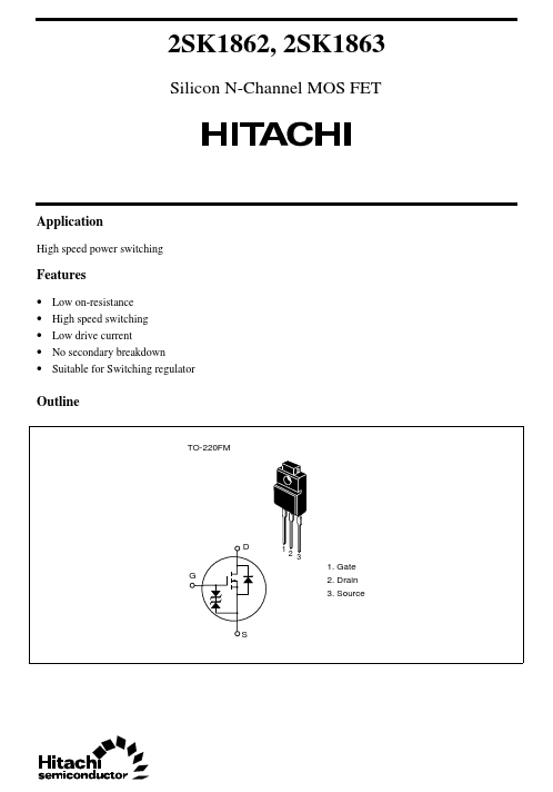
Outline
TO-220FM
2 3
1. Gate 2. Drain 3. Source
2SK1862, 2SK1863
Absolute Maximum Ratings (Ta = 25°C)
Item Drain to source voltage 2SK1862 2SK1863 Gate to source voltage Drain current Drain peak current Body to drain diode reverse drain current Channel dissipation Channel temperature Storage temperature Notes 1. PW ≤ 10 µs, duty cycle ≤ 1 % 2. Value at Tc = 25 °C Symbol VDSS VDSS VGSS ID I D(pulse)- I DR Pch- Tch Tstg
2 1
Ratings 450 500 ±30 3 12 3 25 150
- 55 to +150
Unit V
V A A A W °C °C
2SK1862, 2SK1863
Electrical Characteristics (Ta = 25°C)
Item Drain to source breakdown voltage 2SK1862 2SK1863 V(BR)GSS I GSS I DSS Symbol V(BR)DSS Min 450 500 ±30
- -
- -
- - ±10 250 V µA µA I G = ±100 µA, VDS = 0 VGS = ±25 V, VDS = 0 VDS = 360 V, VGS = 0 VDS = 400 V, VGS = 0 VGS(off) RDS(on) 2.0
- - |yfs| Ciss Coss Crss t d(on) tr t d(off) tf VDF t rr 1.5
- -
- -
- -
- -
- - 2.0 2.2 2.5 330 90 15 7 20 30 20 0.9 300 3.0 2.8 3.0
- -
- -
- -
- -
- - S p F p F p F ns ns ns ns V ns I F = 3 A, VGS = 0 I F = 3 A, VGS = 0, di F / dt = 100 A / µs ID = 2 A VDS = 10 V- 1 VDS = 10 V VGS = 0 f = 1 MHz ID = 2 A VGS = 10 V RL = 15 Ω V Ω I D = 1 m A, VDS = 10 V I D = 2 A, VGS = 10 V- 1 Typ
- Max
- Unit V Test conditions I D = 10 m A, VGS = 0
Gate to source breakdown voltage Gate to source leak current Zero gate voltage drain current 2SK1862 2SK1863
Gate to source cutoff voltage Static drain to source on state resistance 2SK1862...