2SK2685
2SK2685 is GaAs HEMT manufactured by Hitachi Semiconductor.
Features
- Excellent low noise characteristics. Fmin = 0.83 d B Typ. (3 V, 10 m A, 2 GHz)
- High associated gain. Ga = 17 d B Typ. (3 V, 10 m A, 2 GHz)
- High voltage. VDS = 6 or more voltage.
- Small package. (CMPAK-4)
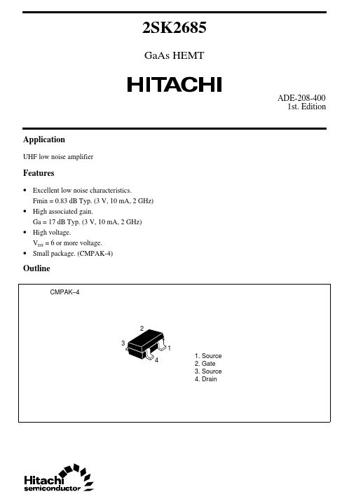
Outline
CMPAK- 4
2 3 4 1 1. Source 2. Gate 3. Source 4. Drain
Absolute Maximum Ratings (Ta = 25°C)
Item Drain to source voltage Gate to source voltage Gate to drain voltage Drain current Channel power dissipation Channel temperature Storage temperature Symbol VDSS VGSO VGDO ID Pch Tch Tstg Ratings 6
- 6
- 7 20 100 125
- 55 to +125 Unit V V V m A m W °C °C
Attention: This device is very sensitive to electro static discharge. It is remended to adopt appropriate cautions when handling this transistor.
Electrical Characteristics (Ta = 25°C)
Item Gate to source leak current Gate to source cutoff voltage Drain current Forward transfer admittance Associated gain Associated gain Associated gain Associated gain Minimum noise figure Minimum noise figure Minimum noise figure Minimum noise figure Note: Marking is “ZT- ”. Symbol I GSS VGS(off) I DSS |yfs| Ga Ga Ga Ga Fmin Fmin Fmin Fmin Min
- - 0.3 35 40
- - 16
- -
- -
- Typ
- - 50 60 17.0 15.2 21.4 19.7 0.83 1.08 0.52 0.74 Max
- 20
- 2.0 70
- -
- -
- -
- 1.0
- Unit µA V m A m S d B d B d B d B d B d B d B d B Test conditions VGS =
- 6 V, VDS = 0 VDS = 3 V, ID = 100 µA VDS = 3 V, VGS = 0 (Pulse Test) VDS = 3 V, ID = 10 m A, f = 1 k Hz VDS = 3 V, ID = 10 m A, f = 2 GHz VDS = 3 V, ID = 3 m A, f = 2 GHz VDS = 3 V, ID = 10 m A, f = 900 MHz VDS = 3 V, ID = 3 m A, f = 900 MHz VDS = 3 V, ID = 10 m A, f = 2 GHz VDS = 3 V, ID = 3 m A, f = 2 GHz VDS = 3 V, ID = 10 m A, f = 900 MHz VDS = 3 V, ID = 3 m A, f = 900 MHz
Typical Output Characteristics Maximum Channel Power Dissipation Curve Channel Power Dissipation Pch (m W) 200 16 150 Drain Current ID (m A) 20
- 0.4
- 0.3 V
- 0.1 V
- 0.5 V
Pulse Test
- 0.6...