2SK3133L
2SK3133L is N-Channel MOSFET manufactured by Hitachi Semiconductor.
Features
- Low on-resistance R DS(on) = 7 mΩ typ.
- Low drive current
- 4 V gate drive device can be driven from 5 V source
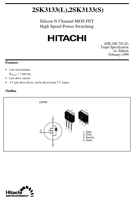
Outline
LDPAK
4 4
D 1 1
1. Gate 2. Drain 3. Source 4. Drain
2SK3133(L),2SK3133(S)
Absolute Maximum Ratings (Ta = 25°C)
Item Drain to source voltage Gate to source voltage Drain current Drain peak current Body-drain diode reverse drain current Channel dissipation Channel temperature Storage temperature Note: 1. PW ≤ 10 µs, duty cycle ≤ 1% 2. Value at Tc = 25°C Symbol VDSS VGSS ID I D(pulse) I DR Pch Tch Tstg
Note 2 Note 1
Ratings 30 ±20 50 200 50 50 150
- 55 to +150
Unit V V A A A W °C °C
Electrical Characteristics (Ta = 25°C)
Item Symbol Min 30
- - 1.0
- - |yfs| Ciss Coss Crss Qg Qgs Qgd t d(on) tr t d(off) tf VDF t rr TBD
- -
- -
- -
- -
- -
- - Typ
- -
- - 7 12 TBD TBD TBD TBD TBD TBD TBD TBD TBD TBD TBD TBD TBD Max
- ±0.1 10 2.5 10 18
- -
- -
- -
- -
- -
- -
- Unit V µA µA V mΩ mΩ S p F p F p F nc nc nc ns ns ns ns V ns I F = 50 A, VGS = 0 I F = 50 A, VGS = 0 di F/ dt = 50 A/ µs Test Conditions I D = 10 m A, VGS = 0 VGS = ±20 V, VDS = 0 VDS = 30 V, VGS = 0 I D = 1 m A, VDS = 10 V Note 1 I D = 25 A, VGS = 10 V Note 1 I D = 25 A, VGS = 4 V Note 1 I D = 25 A, VDS = 10 V Note 1 VDS = 10V VGS = 0 f = 1 MHz VDD = 10 V VGS = 10 V I D = 50 A VGS = 10 V, ID = 25 A RL = 0.4 Ω Drain to source breakdown voltage V(BR)DSS Gate to source leak current Zero gate voltege drain current Gate to source cutoff voltage Static drain to source on state resistance Forward transfer admittance Input capacitance Output capacitance Reverse transfer capacitance Total gate charge Gate to source charge Gate to drain charge Turn-on delay time Rise time Turn-off delay time Fall time Body- drain diode forward voltage Body- drain diode reverse recovery time Note: 1. Pulse test I GSS I DSS VGS(off) RDS(on)
2SK3133(L),2SK3133(S)...