2SK3212
2SK3212 is N-Channel MOSFET manufactured by Hitachi Semiconductor.
Features
- Low on-resistance R DS = 0.1 Ω typ.
- High speed switching
- 4 V gate drive device can be driven from 5 V source
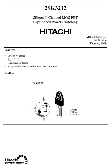
Outline
TO- 220FM
1 2 S
1. Gate 2. Drain 3. Source
Absolute Maximum Ratings (Ta = 25°C)
Item Drain to source voltage Gate to source voltage Drain current Drain peak current Body-drain diode reverse drain current Avalanche current Avalanche energy Channel dissipation Channel temperature Storage temperature Note: Symbol VDSS VGSS ID I D(pulse) I DR I AP
Note3 Note3 Note2 Note1
Ratings 100 ±20 10 40 10 10 10 20 150
- 55 to +150
Unit V V A A A A m J W °C °C
Pch Tch
Tstg
1. PW ≤ 10 µs, duty cycle ≤ 1% 2. Value at Tc = 25°C 3. Value at Tch = 25°C, Rg ≥ 50 Ω
Electrical Characteristics (Ta = 25°C)
Item Symbol Min 100 ±20
- - 1.0
- - 4.5
- -
- -
- -
- -
- Typ
- -
- -
- 100 130 7.5 420 185 100 12 60 105 70 0.9 90 Max
- - ±10 10 2.5 130 180
- -
- -
- -
- -
- - Unit V V µA µA V mΩ mΩ S p F p F p F ns ns ns ns V ns I F = 10 A, VGS = 0 I F = 10 A, VGS = 0 di F/ dt = 50 A/ µs Test Conditions I D = 10 m A, VGS = 0 I G = ±100 µA, VDS = 0 VGS = ±16 V, VDS = 0 VDS = 100 V, VGS = 0 I D = 1 m A, VDS = 10 V I D = 5 A, VGS = 10 VNote4 I D = 5 A, VGS = 4 V Note4 I D = 5 A, VDS = 10 V Note4 VDS = 10 V VGS = 0 f = 1 MHz I D = 5 A, VGS = 10 V RL = 10 Ω Drain to source breakdown voltage V(BR)DSS Gate to source breakdown voltage V(BR)GSS Gate to source leak current Zero gate voltege drain current Gate to source cutoff voltage Static drain to source on state resistance Forward transfer admittance Input capacitance Output capacitance Reverse transfer capacitance Turn-on delay time Rise time Turn-off delay time Fall time Body- drain diode forward voltage Body- drain diode reverse recovery time Note: 4. Pulse test I GSS I DSS VGS(off) RDS(on) RDS(on) |yfs| Ciss Coss Crss t d(on) tr t d(off) tf VDF t rr
Main Characteristics
Power vs. Temperature Derating...