2SK410
2SK410 is N-Channel MOSFET manufactured by Hitachi Semiconductor.
Features
- -
- -
- -
- High breakdown voltage You can decrease handling current. Included gate protection diode No secondary- breakdown Wide area of safe operation Simple bias circuitry No thermal runaway
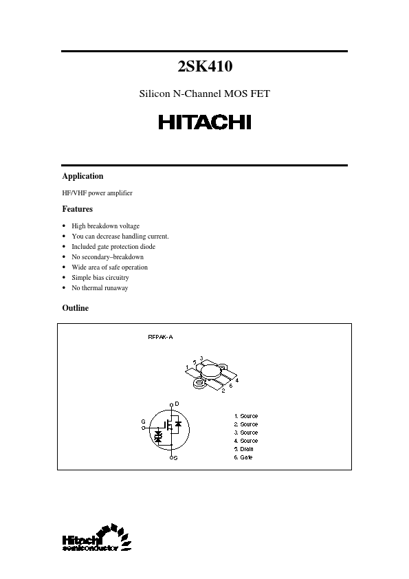
Outline
Absolute Maximum Ratings (Ta = 25°C)
Item Drain to source voltage Gate to source voltage Drain current Channel dissipation Channel temperature Storage temperature Note: 1. Value at TC = 25°C Symbol VDSS VGSS ID Pch- Tch Tstg
Ratings 180 ±20 8 120 150
- 55 to +150
Unit V V A W °C °C
Electrical Characteristics (Ta = 25°C)
Item Power output Drain efficiency Drain to source breakdown voltage Gate to source breakdown voltage Gate to source cutoff voltage Drain current Drain to source saturation voltage Forward transfer admittance Input capacitance Output capacitance Reverse transfer capacitance Power output Power gain Note: 1. Pulse Test Symbol Min PO η V(BR)DSS V(BR)GSS VGS(off) I DSS VDS(on) |yfs| Ciss Coss Crss PO PG 140
- 180 ±20 0.5
- - 0.9
- -
- -
- Typ 180 80
- -
- - 3.8 1.25 440 75 0.5 100 17 Max
- -
- - 3.0 1.0 6.0
- -
- -
- - Unit W % V V V m A V S p F p F p F WPEP d B Test conditions VDD = 80 V, f = 28 MHz, I DQ = 0.1 A, Pin = 5 W I D = 10 m A, VGS = 0 I G = ±100 µA, VDS = 0 I D = 1 m A, VDS = 10 V- 1 VDS = 140 V, VGS = 0 I D = 4 A, VGS = 10 V- 1 I D = 3 A, VDS = 20 V- 1 VGS = 5 V, VDS = 0, f = 1 MHz VGS =
- 5 V, VDS = 50 V, f = 1 MHz VGD =
- 50 V, f = 1 MHz VDD = 80 V, f = 28 MHz, ∆f = 20 k Hz, IMD ≤
- 30 d B
CAUTION: OPERATING HAZARDS Beryllium Oxide Ceramics have been employed in these products. Since dust or fume of the material is highly poison to the human body, please do not treat them mechanically or chemically in the manner which might expose them to the air. And it should never be thrown out with general industrial or domestic waste.
Figure 1 Power vs. Temperature Derating
Figure 2 Maximum Safe Operation Area
Figure 3 Typical Output Characteristics
Figure 4 Typical Transfer Characteristics
Figure 5...