HD74ACT164
HD74ACT164 is Serial-In/ Parallel-Out Shift Register manufactured by Hitachi Semiconductor.
Description
The HD74AC164/HD74ACT164 is a high-speed 8-bit serial-in/parallel-out shift register. Serial data is entered through a 2-input AND gate synchronous with the Low-to-High transition of the clock. The device features an asynchronous Master Reset which clears the register, setting all outputs Low independent of the clock.
Features
- Outputs Source/Sink 24 m A
- HD74ACT164 has TTL-patible Inputs
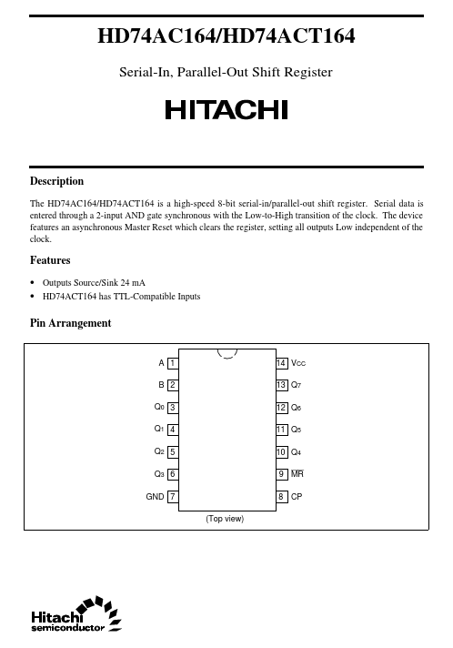
Pin Arrangement
A 1 B 2 Q0 3 Q1 4 Q2 5 Q3 6 GND 7 (Top view)
14 VCC 13 Q7 12 Q6 11 Q5 10 Q4 9 MR 8 CP
HD74AC164/HD74ACT164
Logic Symbol
A B CP MR Q0 Q1 Q2 Q3 Q4 Q5 Q6 Q7
Pin Names
A, B CP MR Q0 to Q7 Data Inputs Clock Pulse Input (Active Rising Edge) Master Reset Input (Active Low) Outputs
Functional Description
The HD74AC164/HD74ACT164 is an edge-triggered 8-bit shift register with serial data entry and an output from each of the eight stages. Data is entered serially through one of two inputs (A or B); either of these inputs can be used as an active High Enable for data entry through the other inputs. An unused input must be tied High. Each Low-to-High transition on the Clock (CP) input shifts data one place to the right and enters into Q 0 the logical AND of the two data inputs (A- B) that existed before the rising clock edge. A Low level on the Master Reset (MR) input overrides all other inputs and clears the register asynchronously, forcing all Q outputs Low.
HD74AC164/HD74ACT164
Mode Select Table
Inputs Operating Mode Reset (Clear) Shift MR L H H H H H L X qn : : : : A X L L H H B X L H L H Outputs Q0 L L L L H Q1 to Q7 L to L q0 to q 6 q0 to q 6 q0 to q 6 q0 to q 6
High Voltage Level Low Voltage Level Immaterial Lower case letters indicate the state of the referenced input or output one setup time prior to the Low-to-High clock transition.
Logic Diagram
A B D CD CP MR Q0 Q1 Q2 Q3 Q4 Q5 Q6 Q7 Q D CD Q D CD Q D CD Q D CD Q D CD Q D CD Q D CD Q
Please note that this diagram is provided only for the understanding of logic operations and should not be...