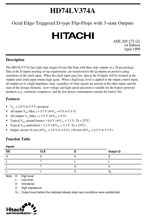
HD74LV374A
HD74LV374A is Octal Edge-Triggered D-type Flip-Flops with 3-state Outputs manufactured by Hitachi Semiconductor.
Description
The HD74LV374A has eight edge trigger D type flip flops with three state outputs in a 20 pin package. Data at the D inputs meeting set up requirements, are transferred to the Q outputs on positive going transitions of the clock input. When the clock input goes low, data at the D inputs will be retained at the outputs until clock input returns high again. When a high logic level is applied to the output control input, all outputs go to a high impedance state, regardless of what signals are present at the other inputs and the state of the storage elements. Low-voltage and high-speed operation is suitable for the battery-powered products (e.g., notebook puters), and the low-power consumption extends the battery life.
Features
- -
- -
- - VCC = 2.0 V to 5.5 V operation All inputs VIH (Max.) = 5.5 V (@VCC = 0 V to 5.5 V) All outputs VO (Max.) = 5.5 V (@VCC = 0 V) Typical VOL ground bounce < 0.8 V (@VCC = 3.3 V, Ta = 25°C) Typical VOH undershoot > 2.3 V (@VCC = 3.3 V, Ta = 25°C) Output current ±8 m A (@VCC = 3.0 V to 3.6 V), ±16 m A (@VCC = 4.5 V to 5.5 V)
Function Table
Inputs OE H L L L Note: H: L: X: Z: Q0 : CLK X ↑ ↑ ↓ D X L H X Output Q Z L H Q0
High level Low level Immaterial High impedance Output level before the indicated steady state input conditions were established.
Pin Arrangement
OE 1 1Q 2 1D 3 2D 4 2Q 5 3Q 6 3D 7 4D 8 4Q 9 GND 10
20 VCC 19 8Q 18 8D 17 7D 16 7Q 15 6Q 14 6D 13 5D 12 5Q 11 CLK
(Top view)
Absolute Maximum Ratings
Item Supply voltage range Input voltage range-
1 1, 2
Symbol VCC VI VO
Ratings
- 0.5 to 7.0
- 0.5 to 7.0
- 0.5 to VCC + 0.5
- 0.5 to 7.0
Unit V V V
Conditions
Output voltage range-
Output: H or L VCC: OFF or Output: Z
Input clamp current Output clamp current Continuous output current Continuous current through VCC or GND Maximum power dissipation at Ta = 25°C (in still air)- 3
I IK I OK IO I CC or IGND PT
- 20 ±50 ±35 ±70 835 757 m A m A m A m A m W
VI < 0 VO < 0 or VO > VCC VO = 0 to...