HD74LV4051A
HD74LV4051A is 8-channel Analog Multiplexer / Demultiplexer manufactured by Hitachi Semiconductor.
Description
The HD74LV4051A handles both analog and digital signals, and enables signals of either type with amplitudes of up to 5.5 V (peak) to be transmitted in either direction (at VCC = 0 V to 5.5 V). Applications include signal gating, chopping, modulation or demodulation (modem), and signal multiplexing for analog-to-digital and digital-to-analog conversion systems.
Features
- VCC = 2.0 V to 5.5 V operation
- All inputs VIH (Max.) = 5.5 V (@VCC = 0 V to 5.5 V)
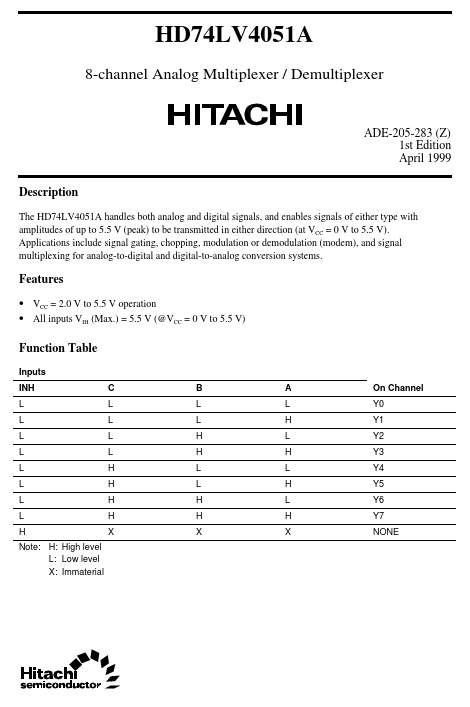
Function Table
Inputs INH L L L L L L L L H Note: H: High level L: Low level X: Immaterial C L L L L H H H H X B L L H H L L H H X A L H L H L H L H X On Channel Y0 Y1 Y2 Y3 Y4 Y5 Y6 Y7 NONE
Pin Arrangement
Y4 1 Y6 2 3
16 VCC 15 Y2 14 Y1 13 Y0 12 Y3 11 A 10 B 9 C
Y7 4 Y5 INH GND GND 5 6 7 8
(Top view)
Absolute Maximum Ratings
Item Supply voltage range Input voltage range-
1 1, 2
Symbol VCC VI VO I IK I OK IO I CC or IGND PT
Ratings
- 0.5 to 7.0
- 0.5 to 7.0
- 0.5 to VCC + 0.5
- 20 ±50 ±25 ±50 785 500
Unit V V V m A m A m A m A m W
Conditions
Output voltage range- Input clamp current Output clamp current
Output: H or L VI < 0 VO < 0 or VO > VCC VO = 0 to VCC
Continuous output current Continuous current through VCC or GND Maximum power dissipation at Ta = 25°C (in still air)- 3
SOP TSSOP
Storage temperature
Tstg
- 65 to 150
°C
Notes: The absolute maximum ratings are values which must not individually be exceeded, and furthermore, no two of which may be realized at the same time. 1. The input and output voltage ratings may be exceeded even if the input and output clamp-current ratings are observed. 2. This value is limited to 5.5 V maximum. 3. The maximum package power dissipation was calculated using a junction temperature of 150°C.
Remended Operating Conditions
Item Supply voltage range Input voltage range Output voltage range Input transition rise or fall rate Symbol VCC VI VI/O ∆t /∆v Min 2.0- 0 0 0 0 0 Operating free-air temperature Ta
- 40
Max 5.5 5.5 VCC 200...