HD74LV4066A
HD74LV4066A is Quad. Analog Switches / Quad. Multiplexers manufactured by Hitachi Semiconductor.
Description
The HD74LV4066A handles both analog and digital signals, and enables signals of either type with amplitudes of up to 5.5 V (peak) to be transmitted in either direction (at VCC = 0 V to 5.5 V). Each switch section has its own enable input control (C). A high-level voltage applied to C turns on the associated switch section. Applications include signal gating, chopping, modulation or demodulation (modem), and signal multiplexing for analog-to-digital and digital-to-analog conversion systems.
Features
- VCC = 2.0 V to 5.5 V operation
- All inputs VIH (Max.) = 5.5 V (@VCC = 0 V to 5.5 V)
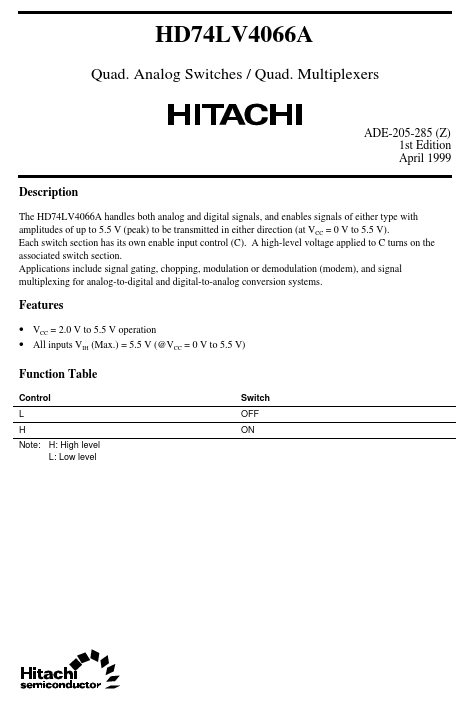
Function Table
Control L H Note: H: High level L: Low level Switch OFF ON
Pin Arrangement
1A 1 1B 2B 2 3
14 VCC 13 1C 12 4C 11 4A 10 4B 9 3B 8 3A
2A 4 2C 3C GND 5 6 7
(Top view)
Absolute Maximum Ratings
Item Supply voltage range Input voltage range-
1 1, 2
Symbol VCC VI VO I IK I OK IO I CC or IGND PT
Ratings
- 0.5 to 7.0
- 0.5 to 7.0
- 0.5 to VCC + 0.5
- 20 ±50 ±25 ±50 785 500
Unit V V V m A m A m A m A m W
Conditions
Output voltage range- Input clamp current Output clamp current
Output: H or L VI < 0 VO < 0 or VO > VCC VO = 0 to VCC
Continuous output current Continuous current through VCC or GND Maximum power dissipation at Ta = 25°C (in still air)- 3
SOP TSSOP
Storage temperature
Tstg
- 65 to 150
°C
Notes: The absolute maximum ratings are values which must not individually be exceeded, and furthermore, no two of which may be realized at the same time.. 1. The input and output voltage ratings may be exceeded even if the input and output clamp-current ratings are observed. 2. This value is limited to 5.5 V maximum. 3. The maximum package power dissipation was calculated using a junction temperature of 150°C.
Remended Operating Conditions
Item Supply voltage range Input voltage range Output voltage range Input transition rise or fall rate Symbol VCC VI VI/O ∆ t/∆ v Min 2.0- 0 0 0 0 0 Operating free-air temperature Ta
- 40
Max 5.5 5.5...