HD74LVC00
HD74LVC00 is Quad. 2-input NAND Gates manufactured by Hitachi Semiconductor.
Description
The HD74LVC00 has four 2-input NAND gates in a 14 pin package. Low voltage and high speed operation is suitable at the battery drive product (note type personal puter) and low power consumption extends the life of a battery for long time operation.
Features
- -
- -
- VCC = 2.0 V to 5.5 V All inputs VIH (Max.) = 5.5 V (@VCC = 0 V to 5.5 V) Typical VOL ground bounce < 0.8 V (@VCC = 3.3 V, Ta = 25°C) Typical VOH undershoot > 2.0 V (@VCC = 3.3 V, Ta = 25°C) High output current ±24 m A (@VCC = 3.0 V to 5.5 V)
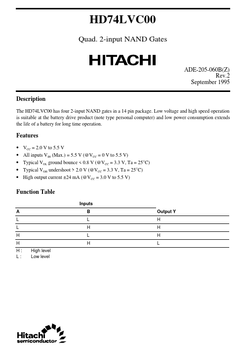
Function Table
Inputs A L L H H H: L: High level Low level B L H L H Output Y H H H L
Pin Arrangement
1A 1 1B 1Y 2 3
14 VCC 13 4B 12 4A 11 4Y 10 3B 9 3A 8 3Y
2A 4 2B 2Y 5 6
GND 7
(Top view)
Absolute Maximum Ratings
Item Supply voltage Input diode current Input voltage Output diode current Symbol VCC I IK VI I OK Ratings
- 0.5 to 6.0
- 50
- 0.5 to 6.0
- 50 50 Output voltage Output current VCC, GND current / pin Storage temperature VO IO I CC or IGND Tstg
- 0.5 to VCC+0.5 ±50 100
- 65 to +150 Unit V m A V m A m A V m A m A °C VO =
- 0.5 V VO = VCC+0.5 V VI =
- 0.5 V Conditions
Note: The absolute maximum ratings are values which must not individually be exceeded, and furthermore, no two of which may be realized at the same time.
Remended Operating Conditions
Item Supply voltage Symbol VCC Ratings 1.5 to 5.5 2.0 to 5.5 Input / Output voltage VI VO Operating temperature Output current Ta I OH 0 to 5.5 0 to V CC
- 40 to 85
- 12
- 24- I OL
1 2
Unit V V V V °C m A m A m A
Conditions Data retention At operation A, B Y
VCC = 2.7 V VCC = 3.0 V to 5.5 V VCC = 2.7 V VCC = 3.0 V to 5.5 V
12 24-
2 m A ns/V
Input rise / fall time
- t r, t f
Notes: 1. This item guarantees maximum limit when one input switches. Waveform : Refer to test circuit of switching characteristics. 2. duty cycle ≤...