J117
J117 is Silicon P-Channel MOS FET manufactured by Hitachi Semiconductor.
Features
- -
- - High speed switching Good frequency characteristics Wide area of safe operation Suitable for switching regulator, DC-DC converter and ultrasonic power oscillators.
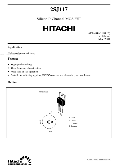
Outline
TO-220AB
3 1. Gate 2. Drain (Flange) 3. Source
2SJ117
Absolute Maximum Ratings (Ta = 25°C)
Item Drain to source voltage Gate to source voltage Drain current Drain peak current Body to drain diode reverse drain current Channel dissipation Channel temperature Storage temperature Notes: 1. Value at TC = 25°C
..
Symbol VDSS VGSS ID I D(pulse) I DR Pch- Tch Tstg
Ratings
- 400 ±20
- 2
- 4
- 2 40 150
- 55 to +150
Unit V V A A A W °C °C
Electrical Characteristics (Ta = 25°C)
Item Drain to source breakdown voltage Gate to source leak current Symbol Min V(BR)DSS I GSS
- 400
- -
- 2.0
- Typ
- -
- - 5 Max
- ±1
- 1
- 5.0 7 Unit V µA m A V Test conditions I D =
- 10 m A, VGS = 0 VGS = ±20 V, VDS = 0 VDS =
- 320 V, VGS = 0 I D =
- 1 m A, VDS =
- 10 V I D =
- 1 A, VGS =
- 15 V- 1 S p F p F p F ns ns ns ns V ns I F =
- 1 A, VGS = 0 I F...