TBB1004
TBB1004 is Twin Build in Biasing Circuit MOS FET IC manufactured by Hitachi Semiconductor.
Features
- -
- - Small SMD package CMPAK-6 built in twin BBFET; To reduce using parts cost & PC board space. Suitable for World Standard Tuner RF amplifier. Very useful for total tuner cost reduction. Withstanding to ESD; Build in ESD absorbing diode. Withstand up to 200V at C=200p F, Rs=0 conditions.
- Provide mini mold packages; CMPAK-6
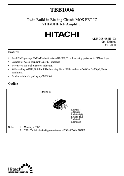
Outline
CMPAK-6
.Data Sheet.co.kr
2 1
1. Drain(1) 2. Source 3. Gate-1(1) 4. Gate-1(2) 5. Gate-2 6. Drain(2)
Notes:
1. 2.
Marking is “DM”. TBB1004 is individual type number of HITACHI TWIN BBFET.
Datasheet pdf
- http://..net/
Absolute Maximum Ratings (Ta = 25°C)
Item Drain to source voltage Gate1 to source voltage Gate2 to source voltage Drain current Channel power dissipation Channel temperature Storage temperature Symbol VDS VG1S VG2S ID Pch Tch Tstg
- 3
Ratings 6 +6 -0 +6 -0 30 250 150
- 55 to +150
Unit V V V m A m W °C °C
Notes: 3. Value on the glass epoxy board (49mm × 38mm × 1mm).
Electrical Characteristics (Ta = 25°C)
The below specification are applicable for UHF unit (FET1)
Item Drain to source breakdown voltage Gate1 to source breakdown voltage Gate2 to source breakdown voltage Symbol V(BR)DSS V(BR)G1SS V(BR)G2SS Min 6 +6 +6
- - 0.5 0.5 13 21 1.4 1.0
- 16 Typ
- -
- -
- 0.7 0.7 17 26 1.8 1.4 0.02 21
.Data Sheet.co.kr
Max
- -
- +100 +100 1.0 1.0 21 31 2.2 1.8 0.04
- Unit V V V n A n A V V m A m S p F p F p F d B
Test Conditions I D = 200µA, VG1S = VG2S = 0 I G1 = +10 µA, VG2S = VDS = 0 I G2 = +10 µA, VG1S = VDS = 0 VG1S = +5V, V G2S = VDS = 0 VG2S = +5V, V G1S = VDS = 0 VDS = 5V, VG2S = 4V, ID = 100µA VDS = 5V, VG1S = 5V, ID = 100µA VDS = 5V, VG1 = 5V VG2S = 4V, RG = 100kΩ VDS = 5V, VG1 = 5V, VG2S =4V RG = 100kΩ, f = 1k Hz VDS = 5V, VG1 = 5V VG2S =4V, RG = 100kΩ f = 1MHz VDS = VG1 = 5V, VG2S = 4V RG = 100kΩ, f = 900MHz Zi=S11- , Zo=S22- (:PG) Zi=S11opt (:NF)
Gate1 to source cutoff current I G1SS Gate2 to source cutoff current I G2SS Gate1 to source cutoff voltage VG1S(off) Gate2 to source cutoff voltage...