HI-8482 Datasheet Text
..
February 2001
GENERAL DESCRIPTION
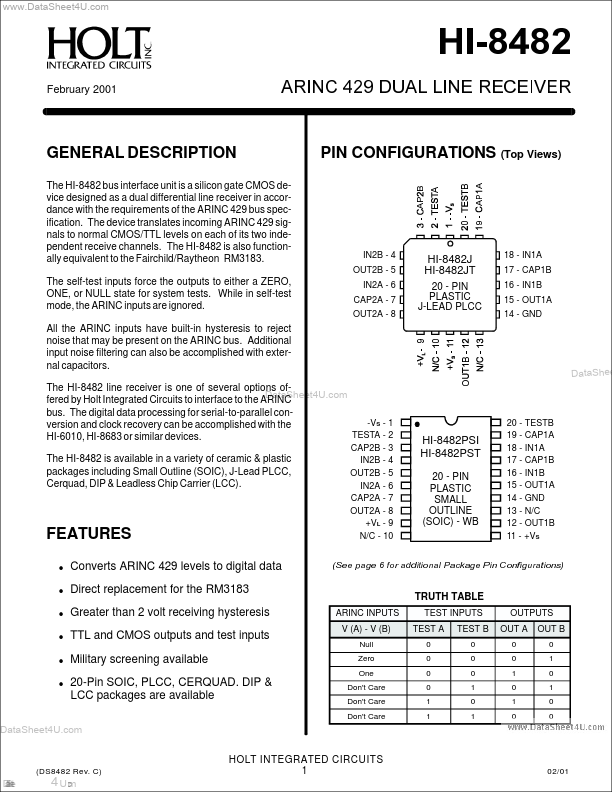
The HI-8482 bus interface unit is a silicon gate CMOS device designed as a dual differential line receiver in accordance with the requirements of the ARINC 429 bus specification. The device translates ining ARINC 429 signals to normal CMOS/TTL levels on each of its two independent receive channels. The HI-8482 is also functionally equivalent to the Fairchild/Raytheon RM3183. The self-test inputs force the outputs to either a ZERO, ONE, or NULL state for system tests. While in self-test mode, the ARINC inputs are ignored. All the ARINC inputs have built-in hysteresis to reject noise that may be present on the ARINC bus. Additional input noise filtering can also be acplished with external capacitors.
PIN CONFIGURATIONS (Top Views)
IN2B
- 4 OUT2B
- 5 IN2A
- 6 CAP2A
- 7 OUT2A
- 8
HI-8482J HI-8482JT
20
- PIN PLASTIC J-LEAD PLCC
18
- IN1A 17
- CAP1B 16
- IN1B 15
- OUT1A 14
- GND
DataShee
The HI-8482 line receiver is one of several options of. fered by Holt Integrated Circuits to interface to the ARINC bus. The digital data processing for serial-to-parallel con-VS
- 1 version and clock recovery can be acplished with the TESTA -2 HI-6010, HI-8683 or similar devices. The HI-8482 is available in a variety of ceramic & plastic packages including Small Outline (SOIC), J-Lead PLCC, Cerquad, DIP & Leadless Chip Carrier (LCC).
CAP2B
- 3 IN2B
- 4 OUT2B
- 5 IN2A
- 6 CAP2A
- 7 OUT2A
- 8 +VL...