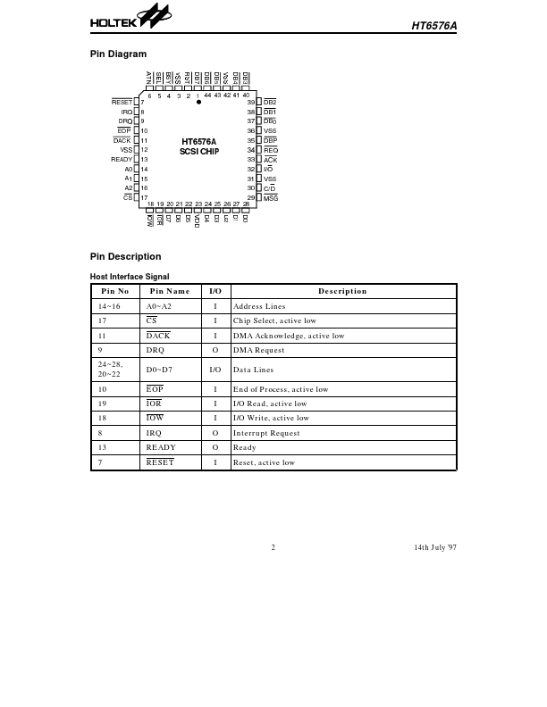
HT6576A Description
Initiator mand register WRITE 7 6 5 4 ASSERT ACK 3 ASSERT BSY 2 ASSERT SEL 1 ASSERT ATN 0 ASSERT DATA ASSERT TRI STATE RESERVED RST BIT 7: ASSERT RST WHEN SET, THE RST SIGNAL IS ASSERTED ON THE SCSI BUS BIT 6: TRI STATE (TEST MODE) BIT.
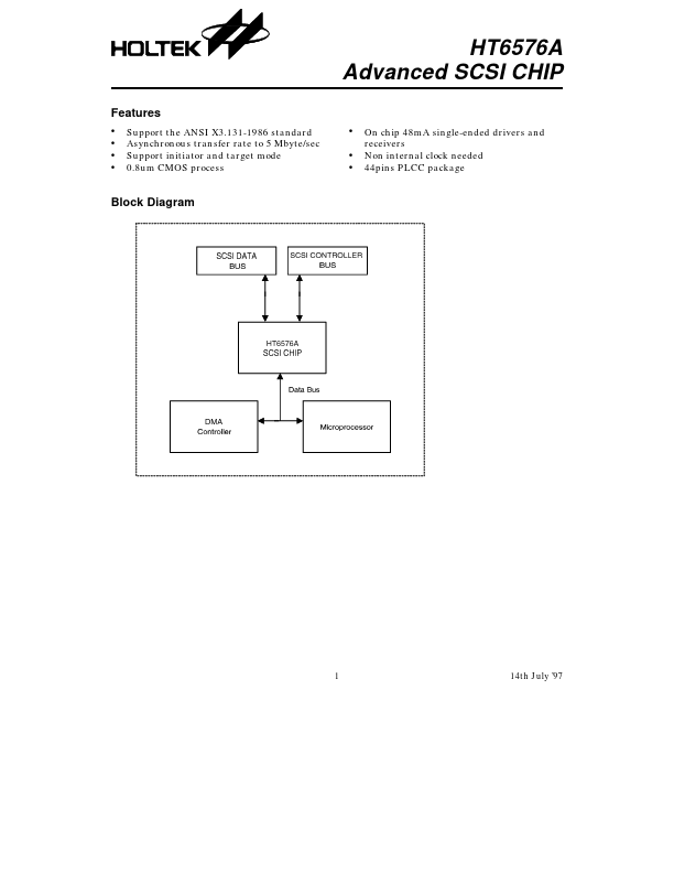
HT6576A Key Features
- Support the ANSI X3.131-1986 standard Asynchronous transfer rate to 5 Mbyte/sec Support initiator and target mode 0.8um
- On chip 48mA single-ended drivers and receivers Non internal clock needed 44pins PLCC package
- BIT 7: ASSERT RST
- BIT 6: TRI-STATE (TEST MODE)
- BIT 5: RESERVED (0)
- BIT 4: ASSERT ACK
- BIT 3: ASSERT BSY
- BIT 2: ASSERT SEL
- BIT 1: ASSERT ATN
- BIT 0: ASSERT DATA