HT82V842
HT82V842 is CCD CDS/PGA/10b-20M-ADC manufactured by Holtek Semiconductor.
HT82V842 CCD CDS/PGA/10b-20M-ADC
Features
- Operating voltage: 2.7V~3.6V
- Low power consumption: 70m W (Typ.)
- Power down mode: less than 30m W
- Accepts a direct signal input to ADC or PGA at 1.0
- Independent ADC input conversion clock and data output clock
- Independent CDS and PGA gain control
- CDS: -1.94/0/6/12d B
- PGA: 0~24d B
- Wide gain range: -1.94~36d B
- High speed sample and hold circuit: pulse width 11ns
VPP (Typ.)
- CCD signal input level: 1.1 VP-P (Max.)
- 10-bit ADC (up to 20MHz)
- Black level neutralizer, target setting: 16~127LSB
- Built-in serial interface
- DNL: ±0.6 LSB (Typ.)
(Min.)
- 48-pin LQFP package
General Description
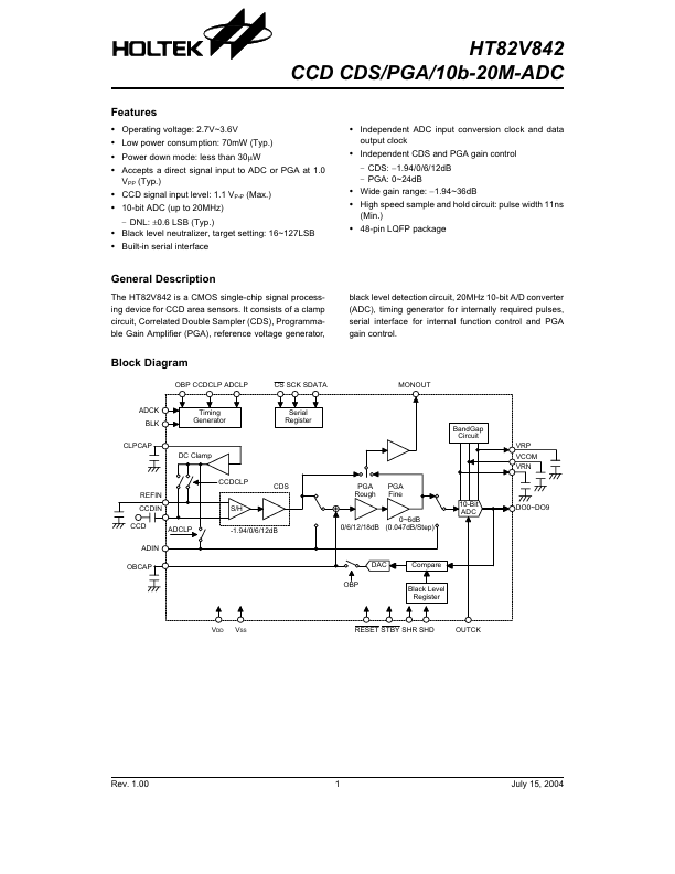
The HT82V842 is a CMOS single-chip signal processing device for CCD area sensors. It consists of a clamp circuit, Correlated Double Sampler (CDS), Programmable Gain Amplifier (PGA), reference voltage generator, black level detection circuit, 20MHz 10-bit A/D converter (ADC), timing generator for internally required pulses, serial interface for internal function control and PGA gain control.
Block Diagram
O B P C C D C L P A D C L P A D C K B L K C L P C A P C S S C K S D A T A M O N O U T
T im in g G e n e ra to r
S e r ia l R e g is te r
B a n d G a p C ir c u it
V R P V C O M V R N
D C C la m p
C C D C L P R E F IN C C D IN C C D A D IN O B C A P O B P D A C C o m p a re B la c k L e v e l R e g is te r A D C L...