Holtek Semiconductor HT2012H
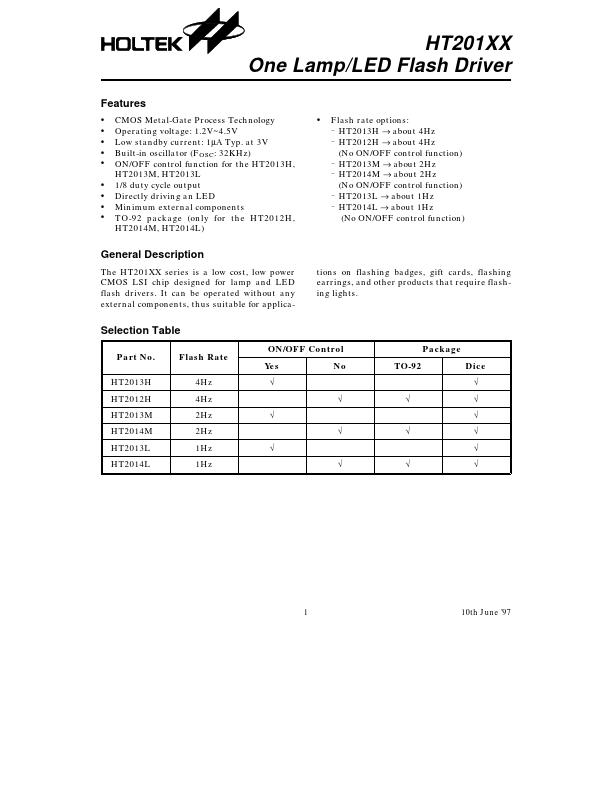
the HT2012H, HT2014M, HT2014L) • Flash rate options: – HT2013H → about 4Hz – HT2012H → about 4Hz (No ON/OFF control function) – HT2013M → about 2Hz – HT2014M → about 2Hz (No ON/OFF control function) – HT2013L → about 1Hz – HT2014L → about 1Hz (No ON/OFF control function) General Description The HT201XX series is a low cost, low power CMOS LSI chip designed for lamp and LED flash drivers. It can be operated without any external components, thus suitable for applications on flashing badges, gift cards, flashing earrings, and other products that require flashing lights.| Part No. | HT2012H |
|---|---|
| Datasheet | HT2012H Download |
| Manufacturer |  Holtek Semiconductor |
| Description | One Lamp/LED Flash Driver |
| Buy | Stock & Price |
FEATURES
●●
●
●
●
●
●
●
● CMOS Metal-Gate Process Technology Operating voltage: 1.2V~4.5V Low standby current: 1µA Typ. at 3V Built-in oscillator (FOSC: 32KHz) ON/OFF control function for the HT2013H, HT2013M, HT2013L 1/8 duty cycle output Directly driving an LED Minimum external components TO-92 package (only for Selection Table Part No. HT2013H HT2012H HT2013M HT2014M HT2013L HT2014L Flash Rate 4Hz 4Hz 2Hz 2Hz 1Hz 1Hz ON/OFF Control Yes √ √ √ √ √ √ √ √ √ Package TO-92 Dice √ √ √ √ √ √ No 1 10th June ’97 HT201XX Pin Assignment Block Diagram Pad Coordinates Pad No. 1 2 3 4 5 Unit: mil X –23.9 –24.13 23.89 13.09 –15.89 Y 13.5 –7.055 13.5 13.5 13.5 Chip size: 60 × 38 (mil)2 *The IC substrate should be connected to VDD in PCB layout artwork. Pad
DESCRIPTION
Pad No. 1 2 3 4 5 Pad Name VDD TEST ON/OFF VSS OUT I/O — — I — O Internal Connection — — CMOS Pull-High — NMOS Open DrainDESCRIPTION
Power supply (positive) For IC test only Lamp/LED flash ON/OFF control pad Power supply (ground) Lamp/LED flash output 2 10th June ’97 HT201XXABSOLUTE MAXIMUM RATINGS
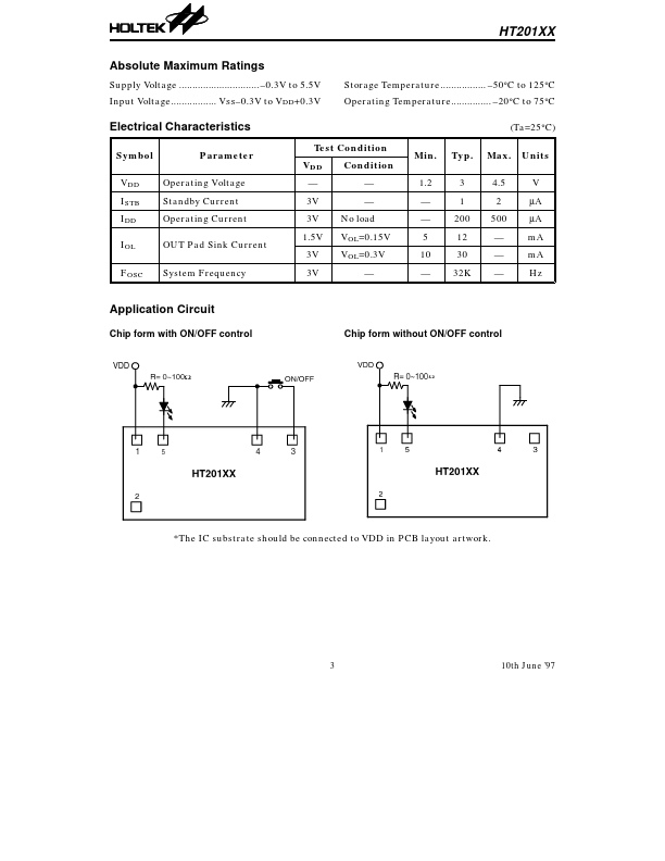
Supply Voltage ..............................–0.3V to 5.5V Input Voltage..........