Datasheet4U Logo Datasheet4U.com
SK Hynix logo

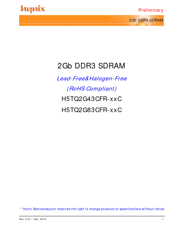
H5TQ2G43CFR-xxC Datasheet

Manufacturer: SK Hynix
H5TQ2G43CFR-xxC datasheet preview

Datasheet Details

Part number H5TQ2G43CFR-xxC
Datasheet H5TQ2G43CFR-xxC_HynixSemiconductor.pdf
File Size 513.41 KB
Manufacturer SK Hynix
Description 2Gb DDR3 SDRAM
H5TQ2G43CFR-xxC page 2 H5TQ2G43CFR-xxC page 3

H5TQ2G43CFR-xxC Overview

Hynix 2Gb DDR3 SDRAMs offer fully synchronous operations referenced to both rising and falling edges of the clock. While all addresses and control inputs are latched on the rising edges of the CK (falling edges of the CK), Data, Data strobes and Write data masks inputs are sampled on both rising and falling edges of it. The data paths are internally pipelined and 8-bit prefetched to achieve very high bandwidth.

H5TQ2G43CFR-xxC Key Features

  • VDD=VDDQ=1.5V +/- 0.075V
  • Fully differential clock inputs (CK, CK) operation
  • Differential Data Strobe (DQS, DQS)
  • BL switch on the fly
  • 8banks
  • Average Refresh Cycle (Tcase of 0 oC~ 95 oC)
  • On chip DLL align DQ, DQS and DQS transition with CK 
  • 7.8 µs at 0oC ~ 85 oC transition
  • 3.9 µs at 85oC ~ 95 oC
  • DM masks write data-in at the both rising and falling 
SK Hynix logo - Manufacturer

More Datasheets from SK Hynix

See all SK Hynix datasheets

Part Number Description
H5TQ2G43AFR-xxC 2Gb DDR3 SDRAM
H5TQ2G43BFR-xxC 2Gb DDR3 SDRAM
H5TQ2G43EFR-xxC 2Gb DDR3 SDRAM
H5TQ2G63BFR-xxC 2Gb DDR3 SDRAM
H5TQ2G63BFR-xxI 2Gb DDR3 SDRAM
H5TQ2G63BFR-xxJ 2Gb DDR3 SDRAM
H5TQ2G63DFR-xxC 2Gb DDR3 SDRAM
H5TQ2G63DFR-xxI 2Gb DDR3 SDRAM
H5TQ2G63DFR-xxJ 2Gb DDR3 SDRAM
H5TQ2G63DFR-xxL 2Gb DDR3 SDRAM

H5TQ2G43CFR-xxC Distributor

Datasheet4U Logo
Since 2006. D4U Semicon. About Datasheet4U Contact Us Privacy Policy Purchase of parts