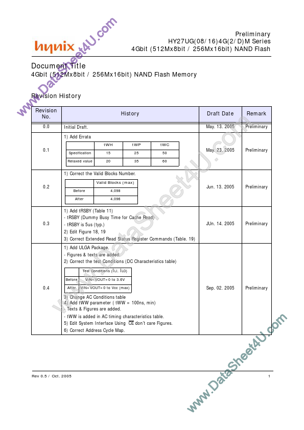
Datasheet4U Logo Datasheet4U.com

HY27UG084G2D - (HY27UGxx Series) 2G-Bit NAND Flash

Download the HY27UG084G2D datasheet PDF. This datasheet also covers the HY27UG084G2M variant, as both devices belong to the same (hy27ugxx series) 2g-bit nand flash family and are provided as variant models within a single manufacturer datasheet.

General Description

The HYNIX HY27UG(08/16)4G(2/D)M series is a 512Mx8bit with spare 16Mx8 bit capacity.

The device is offered in 3.3V Vcc Power Supply.

Its NAND cell provides the most cost-effective solution for the solid state mass storage market.

Key Features

  • 9) Change DC Characteristics (Table 8) - Operating Current ICC1 Typ Before 0.4 After 20 25 Max 40 45 ICC2 Typ 20 25 Max 40 45 ICC3 Typ 20 25 Max 40 45 Sep. 16. 2005 Preliminary 10) Change AC Characteristics - Errata is deleted. tWC Before After 60ns 50ns tWP 35ns 25ns tWH 20ns 15ns - tR is changed. tR Before After 0.5 25us 30us Oct. 05. 2005 Preliminary 1) Delete Concurrent Operation. Rev 0.5 / Oct. 2005 2 Preliminary HY27UG(08/16)4G(2/D)M Series 4Gbit (512Mx8bit / 256Mx16bit) NAND Flash.

📥 Download Datasheet

Note: The manufacturer provides a single datasheet file (HY27UG084G2M_HynixSemiconductor.pdf) that lists specifications for multiple related part numbers.

Datasheet Details

Part number HY27UG084G2D
Manufacturer SK Hynix
File Size 468.31 KB
Description (HY27UGxx Series) 2G-Bit NAND Flash
Datasheet download datasheet HY27UG084G2D Datasheet

Full PDF Text Transcription (Reference)

The following content is an automatically extracted verbatim text from the original manufacturer datasheet and is provided for reference purposes only.

View original datasheet text
w e e Document h Title S / 256Mx16bit) NAND Flash Memory 4Gbit (512Mx8bit a at .D History Revision w w Revision No. 0.0 U 4 t . m o c Preliminary HY27UG(08/16)4G(2/D)M Series 4Gbit (512Mx8bit / 256Mx16bit) NAND Flash History Draft Date May. 13. 2005 Remark Preliminary Initial Draft. 1) Add Errata tWH tWP 25 35 tWC 50 60 0.1 Specification Relaxed value 15 20 May. 23. 2005 1) Correct the Valid Blocks Number. 0.2 Valid Blocks (max) Before After 4,098 4,096 1) Add tRSBY (Table 11) - tRSBY (Dummy Busy Time for Cache Read) 0.3 - tRSBY is 5us (typ.) 2) Edit Figure 18, 19 1) Add ULGA Package. 3) Correct Extended Read Status Register Commands (Table. 19) - Figures & texts are added.