Datasheet4U.com
🌙
HY5DU561622LT SK Hynix Datasheet
Part:
HY5DU561622LT
Description:
(HY5DU56xx22DT) 256Mb DDR SDRAM
Manufacturer:
SK Hynix
Size:
268.63 KB
Download HY5DU561622LT Datasheet PDF
Page 2
Page 3
HY5DU561622LT Key Features
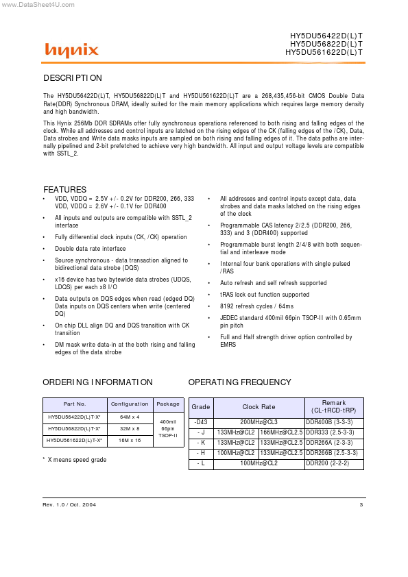
data transaction aligned to bidirectional data strobe (DQS) x16 device has two bytewide data strobes (UDQS, LDQS) per ea
Other HY5DU561622LT Datasheets
Manufacturer
Part Number
Description
SK Hynix
HY5DU561622CTP
256M gDDR SDRAM
×
Close