Datasheet4U Logo Datasheet4U.com

IQX320 - IQX Series

Download the IQX320 datasheet PDF. This datasheet also covers the IQX320_I variant, as both devices belong to the same iqx series family and are provided as variant models within a single manufacturer datasheet.

General Description

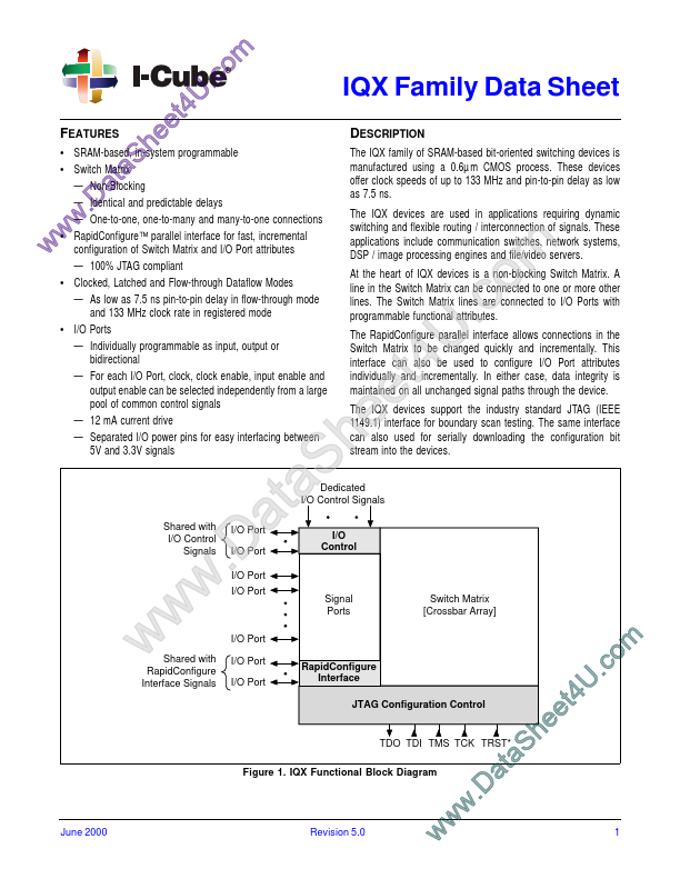
The IQX family of SRAM-based bit-oriented switching devices is manufactured using a 0.6µ m CMOS process.

These devices offer clock speeds of up to 133 MHz and pin-to-pin delay as low as 7.5 ns.

Key Features

  • SRAM-based, in-system programmable.
  • Switch Matrix.
  • Non-Blocking.
  • Identical and predictable delays.
  • One-to-one, one-to-many and many-to-one connections w.
  • RapidConfigure™ parallel interface for fast, incremental configuration of Switch Matrix and I/O Port attributes.
  • 100% JTAG compliant.
  • Clocked, Latched and Flow-through Dataflow Modes.
  • As low as 7.5 ns pin-to-pin delay in flow-through mode and 133 MHz clock rate.

📥 Download Datasheet

Note: The manufacturer provides a single datasheet file (IQX320_I-CUBE.pdf) that lists specifications for multiple related part numbers.

Datasheet Details

Part number IQX320
Manufacturer I-CUBE
File Size 1.45 MB
Description IQX Series
Datasheet download datasheet IQX320 Datasheet

Full PDF Text Transcription (Reference)

The following content is an automatically extracted verbatim text from the original manufacturer datasheet and is provided for reference purposes only.

View original datasheet text
FEATURES • SRAM-based, in-system programmable • Switch Matrix — Non-Blocking — Identical and predictable delays — One-to-one, one-to-many and many-to-one connections w • RapidConfigure™ parallel interface for fast, incremental configuration of Switch Matrix and I/O Port attributes — 100% JTAG compliant • Clocked, Latched and Flow-through Dataflow Modes — As low as 7.5 ns pin-to-pin delay in flow-through mode and 133 MHz clock rate in registered mode • I/O Ports — Individually programmable as input, output or bidirectional — For each I/O Port, clock, clock enable, input enable and output enable can be selected independently from a large pool of common control signals — 12 mA current drive — Separated I/O power pins for easy interfacing between 5V and 3.3V signals w a t a D .