ICS ICS5OSK481
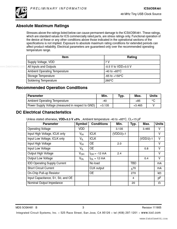
The ICS5OSK481 is a low cost integrated clock synthesizer solution designed for replacing crystals and crystal oscillators. The ICS5OSK481 generates a very accurate 48.00 MHz clock output. External Components Decoupling Capacitor As with any high-performance mixed-signal IC, the ICS5OSK481 must be isolated from system power supply noise to perform optimally.| Part No. | ICS5OSK481 |
|---|---|
| Datasheet | ICS5OSK481 Download |
| Manufacturer |  ICS |
| Description | 48 MHz Tiny USB Clock Source |
| Buy | Stock & Price |
DESCRIPTION
FEATURES
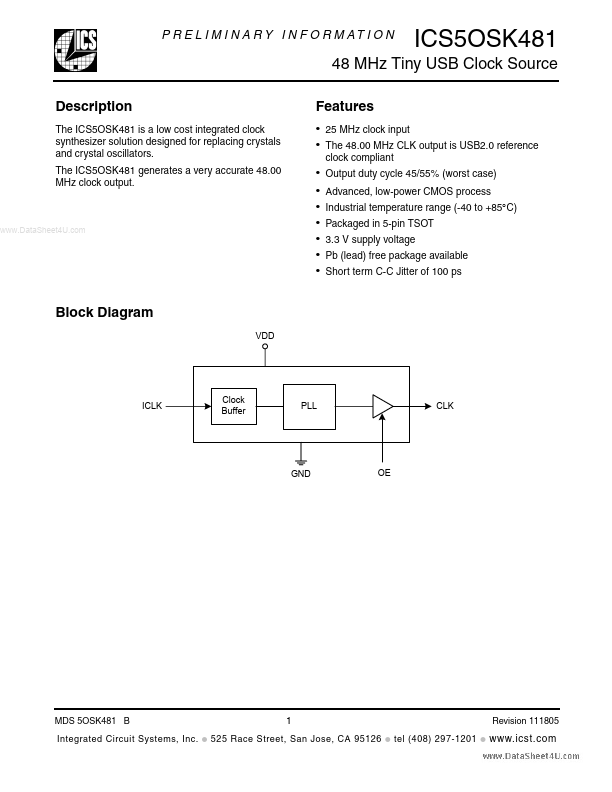
● 25 MHz clock input● The 48.00 MHz CLK output is USB2.0 reference clock compliant
●
●
●
●
●
●
● Output duty cycle 45/55% (worst case) Advanced, low-power CMOS process Industrial temperature range (-40 to +85°C) Packaged in 5-pin TSOT 3.3 V supply voltage Pb (lead) free package available Short term C-C Jitter of 100 ps Block Diagram VDD ICLK Clock Buffer PLL CLK GND OE MDS 5OSK481 B Integrated Circuit Systems, Inc.
● 1 525 Race Street, San Jose, CA 95126
● Revision 111805 tel (408) 297-1201
● P R E L I M I N A R Y I N F O R M AT I O N ICS5OSK481 48 MHz Tiny USB Clock Source Pin Assignment ICLK GND CLK 1 2 3 4 VDD 5 OE Pin Descriptions Pin Number 1 2 3 4 5 Pin Name ICLK GND CLK VDD OE Pin Type Input Power Output Power Input Pin
DESCRIPTION
25 MHz clock input. Connect to a parallel resonant fundamental crystal or input clock. Connect to ground. PLL output clock. Internal pull-down resistor. Connect to 3.3 V. Output Enable pin. Internal pull-up resistor. OE=0 outputs tristate with weak pull-down.