ICS ICS87973I-147
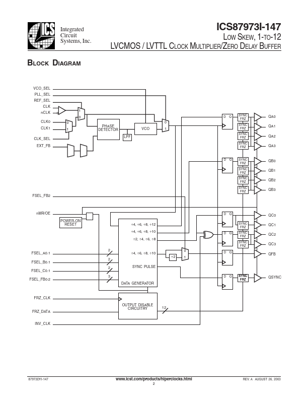
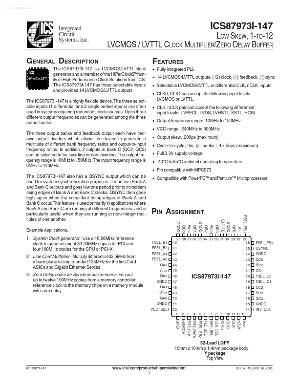
The ICS87973I-147 is a LVCMOS/LVTTL clock generator and a member of the HiPerClockS™family of High Performance Clock Solutions from ICS. The ICS87973I-147 has three selectable inputs and provides 14 LVCMOS/LVTTL outputs. The ICS87973I-147 is a highly flexible device.| Part No. | ICS87973I-147 |
|---|---|
| Datasheet | ICS87973I-147 Download |
| Manufacturer |  ICS |
| Description | 1-TO-12 LVCMOS / LVTTL CLOCK MULTIPLIER/ZERO DELAY BUFFER |
| Buy | Stock & Price |
FEATURES
● Fully integrated PLL● 14 LVCMOS/LVTTL outputs; (12) clock, (1) feedback, (1) sync
● Selectable LVCMOS/LVTTL or differential CLK, nCLK inputs
● CLK0, CLK1 can accept the following input levels: LVCMOS or LVTTL
● CLK, nCLK pair can accept the following differential input levels: LVPECL, LVDS, LVHSTL, SSTL, HCSL
● Output frequency range: 10MHz to 150MHz
● VCO range: 240MHz to 500MHz
● Output skew: 200ps (maximum)
● Cycle-to-cycle jitter, (all banks ÷ 4): 55ps (maximum)
● Full 3.3V supply voltage
● -40°C to 85°C ambient operating temperature
● Pin compatible with MPC973
● Compatible with PowerPC™ and Pentium™ Microprocessors
GENERAL DESCRIPTION
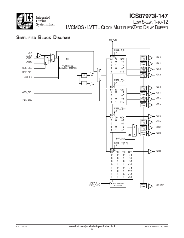
ICS HiPerClockS™ The ICS87973I-147 is a highly flexible device. The three selectable inputs (1 differential and 2 single ended inputs) are often used in systems requiring redundant clock sources. Up to three different output frequencies can be generated among the three output banks. The three output banks and feedback output each have their own output dividers which allows the device to generate a multitude of different bank frequency ratios and output-to-input frequency ratios.