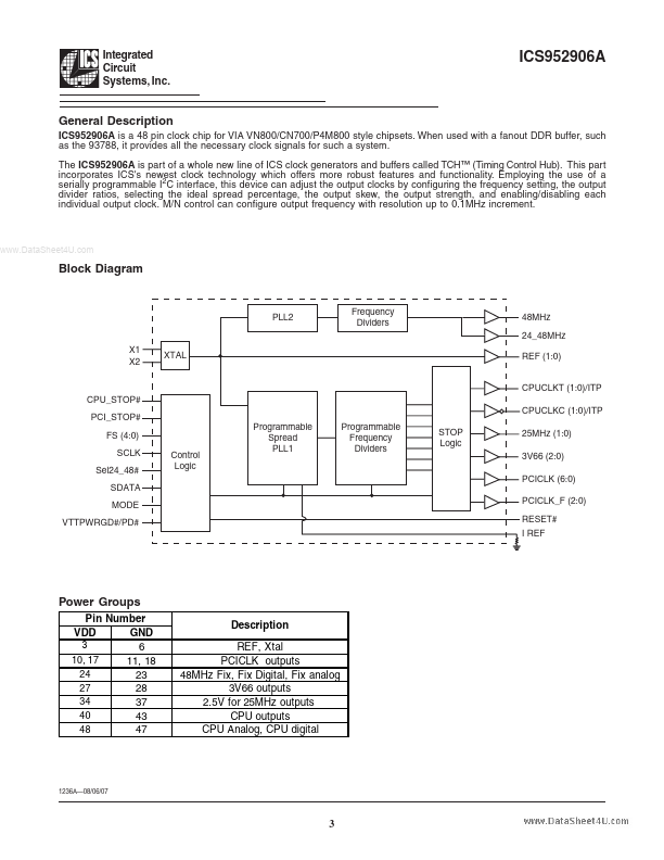
Datasheet4U Logo Datasheet4U.com

ICS952906A - Programmable Timing Control Hub

Description

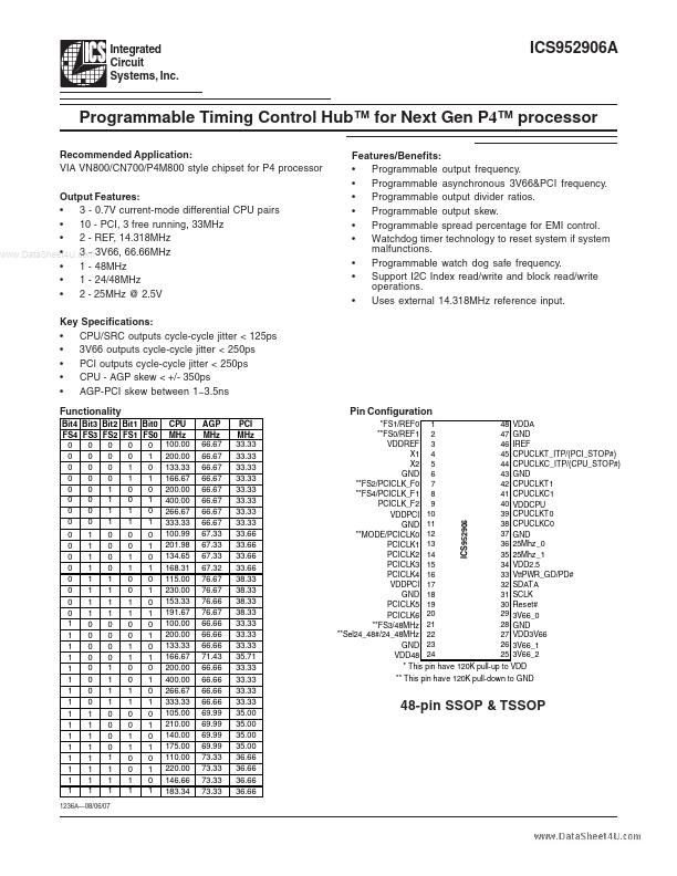
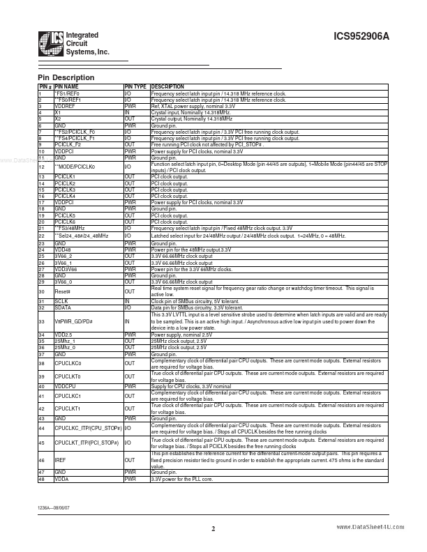
PIN # 1 2 3 4 5 6 7 8 9 10 11 12 13 14 15 16 17 18 19 20 21 22 23 24 25 26 27 28 29 30 31 32 33 34 35 36 37 38 39 40 41 42 43 44 45 PIN NAME FS1/REF0 FS0/REF1 VDDREF X1 X2 GND FS2/PCICLK_F0 FS4/PCICLK_F1 PCICLK_F2 VDDPCI GND MODE/PCICLK0 PCICLK1 PCICLK2 P

Features

  • 3 - 0.7V current-mode differential CPU pairs.
  • 10 - PCI, 3 free running, 33MHz.
  • 2 - REF, 14.318MHz.
  • 3 - 3V66, 66.66MHz www. DataSheet4U. com.
  • 1 - 48MHz.
  • 1 - 24/48MHz.
  • 2 - 25MHz @ 2.5V Key Specifications:.
  • CPU/SRC outputs cycle-cycle jitter < 125ps.
  • 3V66 outputs cycle-cycle jitter < 250ps.
  • PCI outputs cycle-cycle jitter < 250ps.
  • CPU - AGP skew < +/- 350ps.
  • AGP-PCI skew between 1~3.5ns Functi.

📥 Download Datasheet

Datasheet preview – ICS952906A

Datasheet Details

Part number ICS952906A
Manufacturer ICS
File Size 350.60 KB
Description Programmable Timing Control Hub
Datasheet download datasheet ICS952906A Datasheet
Additional preview pages of the ICS952906A datasheet.
Other Datasheets by ICS

Full PDF Text Transcription

Click to expand full text
Integrated Circuit Systems, Inc. ICS952906A Programmable Timing Control Hub™ for Next Gen P4™ processor Recommended Application: VIA VN800/CN700/P4M800 style chipset for P4 processor Output Features: • 3 - 0.7V current-mode differential CPU pairs • 10 - PCI, 3 free running, 33MHz • 2 - REF, 14.318MHz • 3 - 3V66, 66.66MHz www.DataSheet4U.com • 1 - 48MHz • 1 - 24/48MHz • 2 - 25MHz @ 2.5V Key Specifications: • CPU/SRC outputs cycle-cycle jitter < 125ps • 3V66 outputs cycle-cycle jitter < 250ps • PCI outputs cycle-cycle jitter < 250ps • CPU - AGP skew < +/- 350ps • AGP-PCI skew between 1~3.5ns Functionality Bit4 Bit3 Bit2 Bit1 Bit0 CPU FS4 FS3 FS2 FS1 FS0 MHz 100.00 0 0 0 0 0 200.00 0 0 0 0 1 133.33 0 0 0 1 0 166.67 0 0 0 1 1 0 0 1 0 0 200.00 0 0 1 0 1 400.00 0 0 1 1 0 266.67 0 0 1 1 1 333.
Published: |