ICS ICSSSTUBF32866A
This 25-bit 1:1 or 14-bit 1:2 configurable registered buffer is designed for 1.7-V to 1.9-V VDD operation. The control inputs are LVCMOS.| Part No. | ICSSSTUBF32866A |
|---|---|
| Datasheet | ICSSSTUBF32866A Download |
| Manufacturer |  ICS |
| Description | 25-Bit Configurable Registered Buffer |
| Buy | Stock & Price |
FEATURES
:● 25-bit 1:1 or 14-bit 1:2 configurable registered buffer with parity check functionality
● Supports SSTL_18 JEDEC specification on data inputs and outputs
● Supports LVCMOS switching levels on CSR and RESET inputs
● Low voltage operation VDD = 1.7V to 1.9V
● Available in 96 BGA package
● Drop-in replacement for ICSSSTUA32864
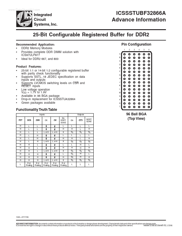
● Green packages available Pin Configuration 1 A B C D E F G H J K L M N P R T 2 3 4 5 6 Functionality Truth Table I nputs RST H H H H H H H H H H H H L DCS L L L L L L H H H H H H X or Floating CSR L L L H H H L L L H H H X or Floating L or H X or Floating L or H X or Floating L or H L or H L or H L or H L or H L or H CK CK Dn, DODT, DCK E L H X L H X L H X L H X X or Floating Qn L H Q0 L H Q0 L H Q0 Q0 Q0 Q0 L Outputs QCS L L Q0 L L Q0 H H Q0 H H Q0 L QODT, QCKE L H Q0 L H Q0 L H Q0 L H Q0 L 96 Ball BGA (Top View) 1240—07/17/06 ADVANCE INFORMATION documents contain information on products in the formative or design phase development. Characteristic data and other specifications are design goals.

