MK2304-2
MK2304-2 is LOW SKEW BUFFER manufactured by ICS.
Features
- -
- -
- -
- Packaged in 8 pin SOIC Zero input-output delay Two 1X outputs plus two 1/2X outputs Output to output skew is less than 200 ps Output clocks up from 10 MHz to 133 MHz at 3.3 V Ability to generate 2X the input Full CMOS outputs with 18 m A output drive capability at TTL levels at 3.3 V spectrum clock generators
Description
The MK2304-2 is a low jitter, low skew, high performance Phase Lock Loop (PLL) based zero delay buffer for high speed applications. Based on ICS’ proprietary low jitter PLL techniques, the device provides four low skew outputs at speeds up to 133 MHz at 3.3 V. The MK2304-2 includes a bank of two outputs running at 1/2X. In the zero delay mode, the rising edge of the input clock is aligned with the rising edges of all 4 outputs. pared to petitive CMOS devices, the MK2304-2 has the lowest jitter. The MK2304-2 PLL enters a power-down state when there are no rising edges on the REF input. In this mode, all outputs are tri-stated and the PLL is turned off, resulting in leass than 25 µA of current draw. ICS manufactures the largest variety of clock generators and buffers and is the largest clock supplier in the world.
- Spread Smart TM technology works with spread
- -
- -
- Advanced, low power, sub micron CMOS process Operating voltage of 3.3 V Available in industial temperature operation Available in Pb (lead) free package Low Standby Current
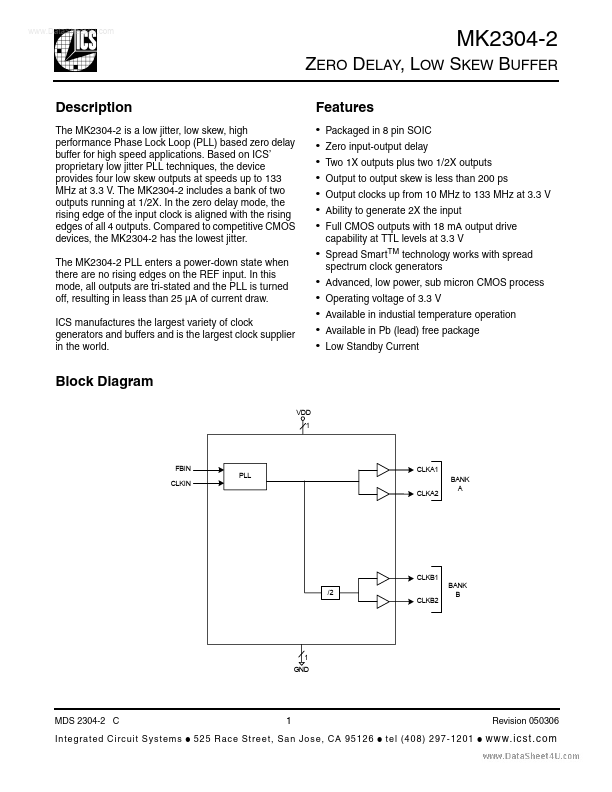
Block Diagram
VDD 1
FBIN CLKIN
CLKA1 CLKA2 BANK A
CLKB1 /2 CLKB2 BANK B
1 GND
MDS 2304-2 C I n t e gra te d C i r c u i t S y s t e m s
- 1
525 Race Stre et, San Jo se, CA 9 5126
- Revision 050306 te l (40 8) 2 97-12 01
- w w w. i c st . c o m
..
MK2304-2 ZERO DELAY, LOW SKEW BUFFER
Pin Assignment
Feedback Configuration Table
Feedback From Bank A Bank B CLKA1:A2 CLKIN 2XCLKIN CLKB1:B2 CLKIN/2 CLKIN
REF CLKA1 CLKA2 GND
1 2 3 4
8 7 6 5
FBK VDD CLKB2 CLKB1
8 Pi n ( 150 mi l ) SOI C
Pin Descriptions
Pin Number 1 2 3 4 5 6 7 8 Pin Name REF CLKA1 CLKA2 GND CLKB1 CLKB1 VDD...