ICS V385A
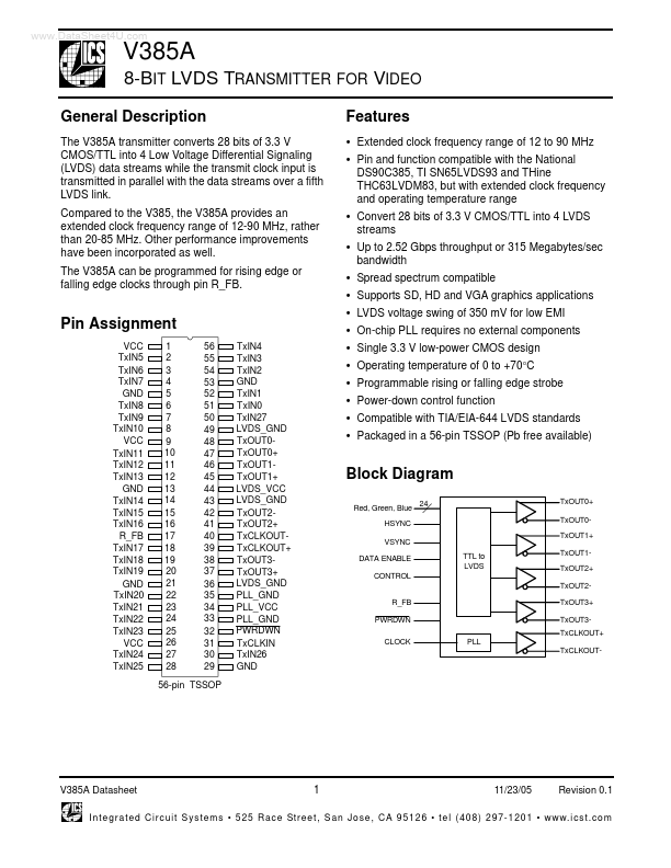
The V385A transmitter converts 28 bits of 3.3 V CMOS/TTL into 4 Low Voltage Differential Signaling (LVDS) data streams while the transmit clock input is transmitted in parallel with the data streams over a fifth LVDS link. The V385A can be programmed for rising edge or falling edge clocks through pin R_FB. Compared to the V385, the V385A provides an extended clock frequency range of 12-90 MHz, rather than 20-85 MHz.| Part No. | V385A |
|---|---|
| Datasheet | V385A Download |
| Manufacturer |  ICS |
| Description | 8-BIT LVDS TRANSMITTER |
| Buy | Stock & Price |
GENERAL DESCRIPTION
Other performance improvements have been incorporated as well.FEATURES
● Extended clock frequency range of 12 to 90 MHz● Pin and function compatible with the National DS90C385, TI SN65LVDS93 and THine THC63LVDM83, but with extended clock frequency and operating temperature range
● Convert 28 bits of 3.3 V CMOS/TTL into 4 LVDS streams
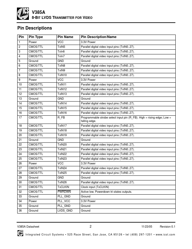
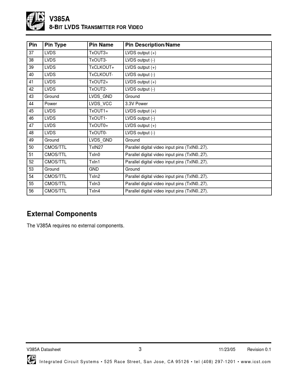
● Up to 2.52 Gbps throughput or 315 Megabytes/sec bandwidth Pin Assignment VCC TxIN5 TxIN6 TxIN7 GND TxIN8 TxIN9 TxIN10 VCC TxIN11 TxIN12 TxIN13 GND TxIN14 TxIN15 TxIN16 R_FB TxIN17 TxIN18 TxIN19 GND TxIN20 TxIN21 TxIN22 TxIN23 VCC TxIN24 TxIN25 1 2 3 4 5 6 7 8 9 10 11 12 13 14 15 16 17 18 19 20 21 22 23 24 25 26 27 28 56 55 54 53 52 51 50 49 48 47 46 45 44 43 42 41 40 39 38 37 36 35 34 33 32 31 30 29 TxIN4 TxIN3 TxIN2 GND TxIN1 TxIN0 TxIN27 LVDS_GND TxOUT0TxOUT0+ TxOUT1TxOUT1+ LVDS_VCC LVDS_GND TxOUT2TxOUT2+ TxCLKOUTTxCLKOUT+ TxOUT3TxOUT3+ LVDS_GND PLL_GND PLL_VCC PLL_GND PWRDWN TxCLKIN TxIN26 GND
●
●
●
●
●
●
●
●
●
● Spread spectrum...