ICST ICS542
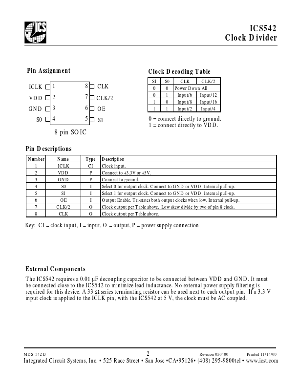
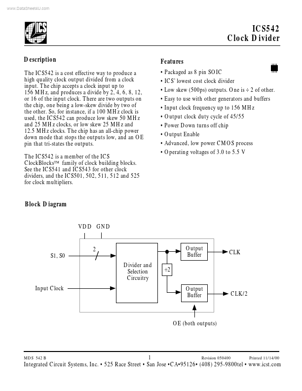
The ICS542 is a cost effective way to produce a high quality clock output divided from a clock input. The chip accepts a clock input up to 156 MHz, and produces a divide by 2, 4, 6, 8, 12, or 16 of the input clock. The chip has an all-chip power down mode that stops the outputs low, and an OE pin that tri-states the outputs.| Part No. | ICS542 |
|---|---|
| Datasheet | ICS542 Download |
| Manufacturer |  ICST |
| Description | Clock Divider |
| Buy | Stock & Price |
DESCRIPTION
There are two outputs on the chip, one being a low-skew divide by two of the other. So, for instance, if a 100 MHz clock is used, the ICS542 can produce low skew 50 MHz and 25 MHz clocks, or low skew 25 MHz and 12.5 MHz clocks. The ICS542 is a member of the ICS ClockBlocks™ family of clock building blocks. See the ICS541 and ICS543 for other clock dividers, and the ICS501, 502, 511, 512 and 525 for clock multipliers.FEATURES
● Packaged as 8 pin SOIC● ICS’ lowest cost clock divider
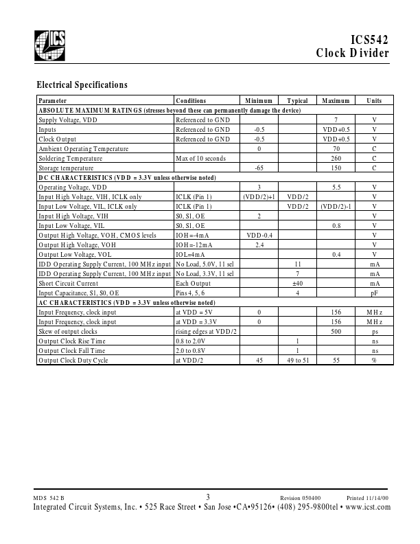
● Low skew (500ps) outputs. One is ÷ 2 of other.
● Easy to use with other generators and buffers
● Input clock frequency up to 156 MHz
● Output clock duty cycle of 45/55
● Power Down turns off chip
● Output Enable
● Advanced, low power CMOS process
● Operating voltages of 3.0 to 5.5 V Block Diagram VDD GND 2 S1, S0 Divider and Selection Circuitry Input Clock ÷2 Output Buffer CLK Output Buffer CLK/2 OE (both outputs) 1 Revision 050400 Printed 11/14/00 Integrated Circuit Systems, Inc.
● 525 Race S...