ICS557-06 Overview
Description
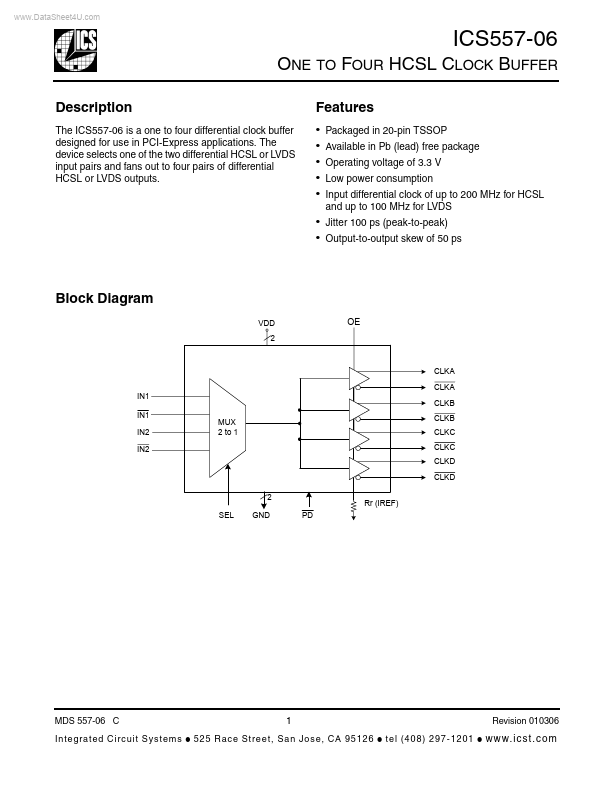
The ICS557-06 is a one to four differential clock buffer designed for use in PCI-Express applications. The device selects one of the two differential HCSL or LVDS input pairs and fans out to four pairs of differential HCSL or LVDS outputs.
Key Features
- Jitter 100 ps (peak-to-peak)
- Output-to-output skew of 50 ps