ICST ICS853001
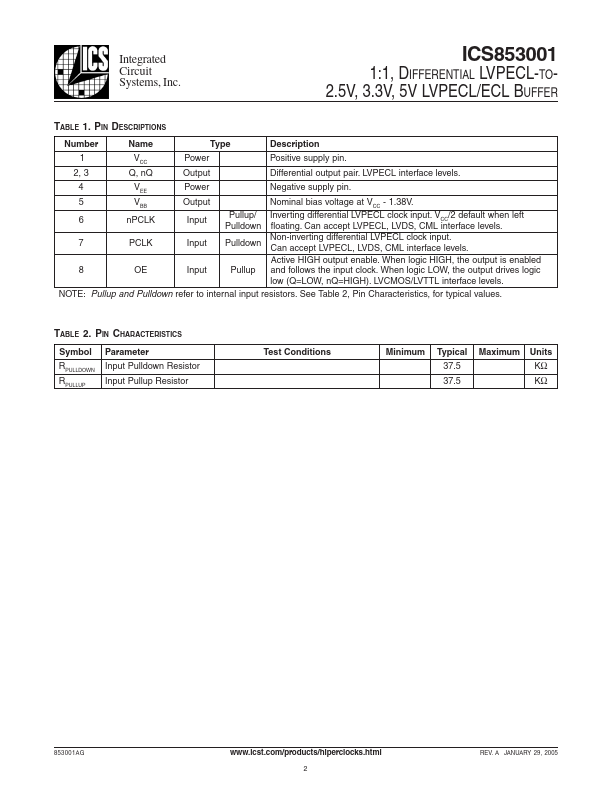
The ICS853001 is a 1:1 Differential LVPECLto-LVPE C L B u f fe r a n d a m e m b e r o f t h e HiPerClockS™ HiPerClock S ™ family of High Perfor mance Clock Solutions from ICS. The ICS853001 may be used to regenerate LVPECL clocks which may have been attenuated, across a long trace, or may also be used as a differential-to-LVPECL translator. The differential input can accept the following differential input types: LVPECL, LVDS and CML.| Part No. | ICS853001 |
|---|---|
| Datasheet | ICS853001 Download |
| Manufacturer |  ICST |
| Description | LVPECL/ECL BUFFER |
| Buy | Stock & Price |
FEATURES
● 1:1 Differential LVPECL-to-LVPECL / ECL buffer● 1 LVPECL clock output pair
● 1 Differential LVPECL PCLK, nPCLK input pair
● PCLK, nPCLK pair can accept the following differential input levels: LVPECL, LVDS, CML
● Maximum output frequency: >2.5GHz
● Part-to-part skew: 100ps (maximum)
● Propagation delay: 500ps (maximum)
● Additive phase jitter, RMS: 0.03ps (typical)
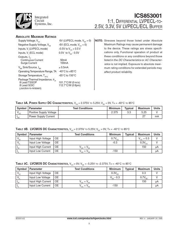
● LVPECL mode operating voltage supply range: VCC = 2.375V to 5.25V, VEE = 0V
● ECL mode operating voltage supply range: VCC = 0V, VEE = -5.25V to -2.375V
● -40°C to 85°C ambient operating temperature
● Lead-Free package RoHS compliant
GENERAL DESCRIPTION
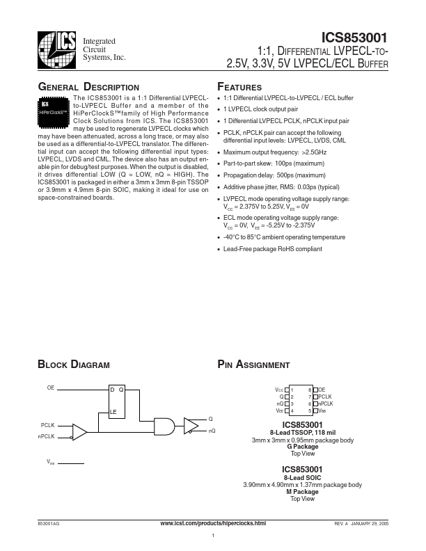
The device also has an output enable pin for debug/test purposes. When the output is disabled, it drives differential LOW (Q = LOW, nQ = HIGH). The ICS853001 is packaged in either a 3mm x 3mm 8-pin TSSOP or 3.9mm x 4.9mm 8-pin SOIC, making it ideal for use on space-constrained boards. ICS BLOCK DIAGRAM OE PIN ASSIGNMENT D Q VCC Q nQ VEE Q 1 2 3 4 8 7 6 5 OE PCLK...