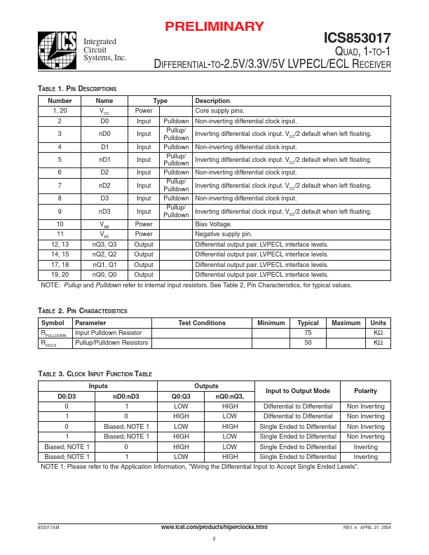
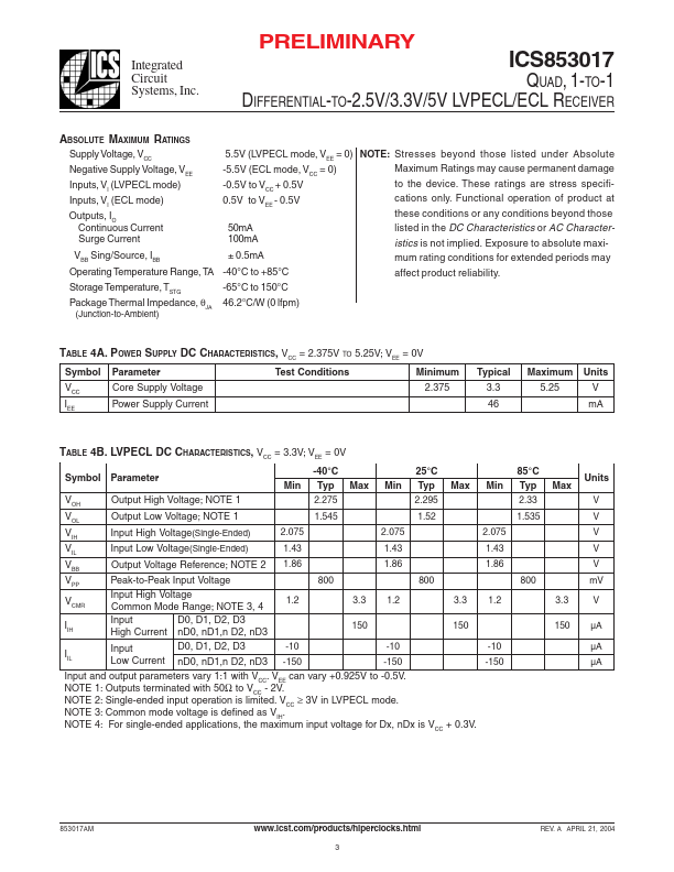
ICST ICS853017
The ICS853017 is a quad 1-to-1, 2.5V/3.3V/5V differential LVPECL/ECL receiver and a member of HiPerClockS™ the HiperclocksTM family of High Performance Clock Solutions from ICS. The ICS853017 operates with a positive or negative power supply at 2.5V, 3.3V or 5V, and can accept both single-ended and differential inputs. For single-ended operation, an internally generated voltage, which is available on output pin VBB, can be used as a switching bias voltage on the unused input of the differential pair.| Part No. | ICS853017 |
|---|---|
| Datasheet | ICS853017 Download |
| Manufacturer |  ICST |
| Description | LVPECL/ECL RECEIVER |
| Buy | Stock & Price |
FEATURES
● 4 differential LVPECL / ECL 1:1 receivers● 4 differential LVPECL clock input pairs
● PCLKx, nPCLKx pairs can accept the following differential input levels: LVPECL, LVDS, CML, SSTL
● Output frequency: >2GHz (typical)
● Translates any single ended input signal to LVPECL levels with resistor bias on nPCLKx input
● Output skew: TBD
● Part-to-part skew: TBD
● Propagation delay: 320ps (typical)
● LVPECL mode operating voltage supply range: VCC = 2.375V to 5.25V
● ECL mode operating voltage supply range: VCC = 0V, VEE = -5.25V to -2.375V
● -40°C to 85°C ambient operating temperature
● Pin compatible with MC100LVEL17
GENERAL DESCRIPTION
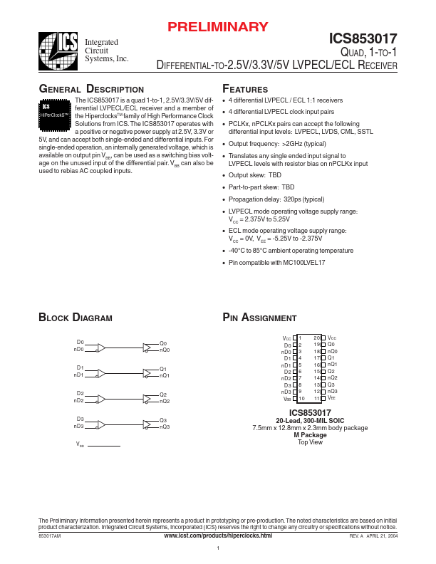
VBB can also be used to rebias AC coupled inputs. ICS BLOCK DIAGRAM D0 nD0 Q0 nQ0 PIN ASSIGNMENT VCC D0 nD0 D1 nD1 D2 nD2 D3 nD3 VBB 1 2 3 4 5 6 7 8 9 10 20 19 18 17 16 15 14 13 12 11 VCC Q0 nQ0 Q1 nQ1 Q2 nQ2 Q3 nQ3 VEE D1 nD1 Q1 nQ1 D2 nD2 Q2 nQ2 D3 nD3 ICS853017 Q3 nQ3 V BB 20-Lead, 300-MIL SOIC 7.5mm x 12.8mm x 2.3mm body package M Package Top View The Preliminary Information presented herein represents a product in prototyping or pre-production.