ICST ICS85322I
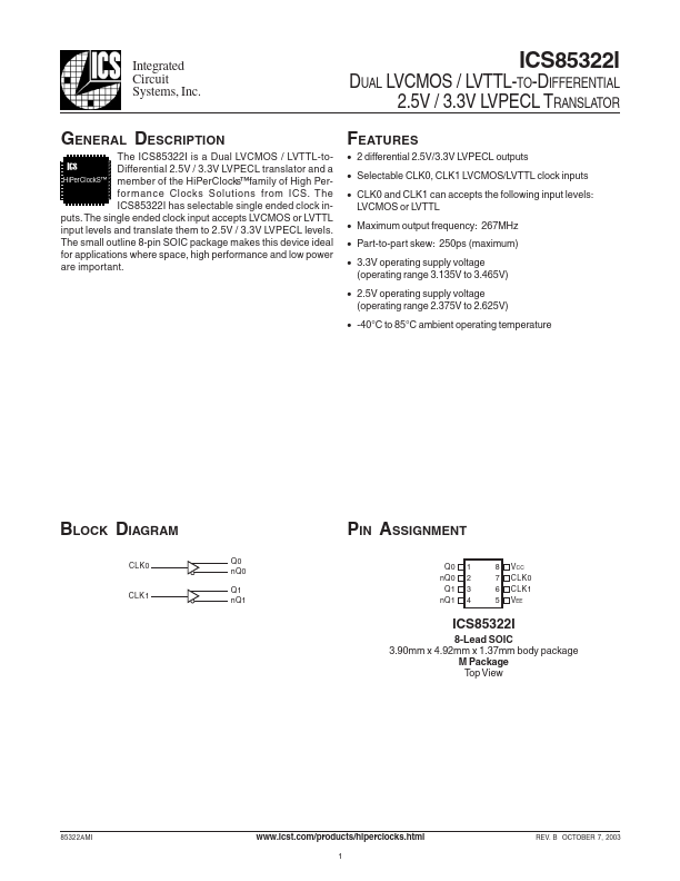
The ICS85322I is a Dual LVCMOS / LVTTL-toDifferential 2.5V / 3.3V LVPECL translator and a HiPerClockS™ member of the HiPerClocks™family of High Perfor mance Clocks Solutions from ICS. The ICS85322I has selectable single ended clock inputs. The single ended clock input accepts LVCMOS or LVTTL input levels and translate them to 2.5V / 3.3V LVPECL levels.| Part No. | ICS85322I |
|---|---|
| Datasheet | ICS85322I Download |
| Manufacturer |  ICST |
| Description | LVPECL TRANSLATOR |
| Buy | Stock & Price |
FEATURES
● 2 differential 2.5V/3.3V LVPECL outputs● Selectable CLK0, CLK1 LVCMOS/LVTTL clock inputs
● CLK0 and CLK1 can accepts the following input levels: LVCMOS or LVTTL
● Maximum output frequency: 267MHz
● Part-to-part skew: 250ps (maximum)
● 3.3V operating supply voltage (operating range 3.135V to 3.465V)
● 2.5V operating supply voltage (operating range 2.375V to 2.625V)
● -40°C to 85°C ambient operating temperature
GENERAL DESCRIPTION
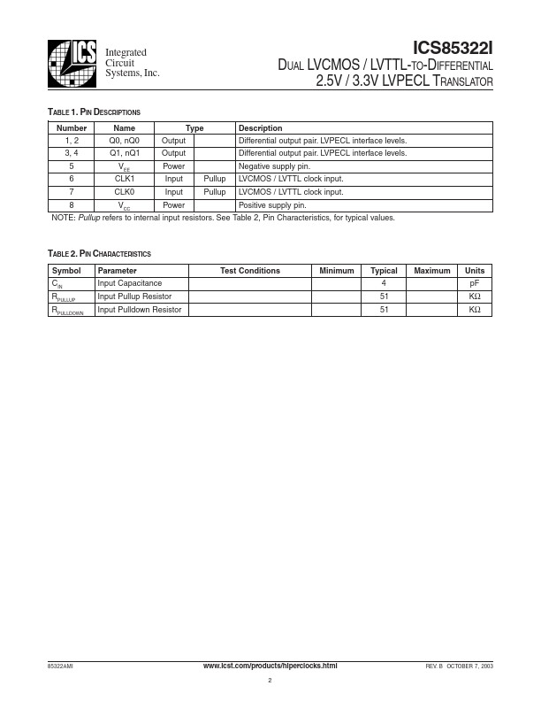
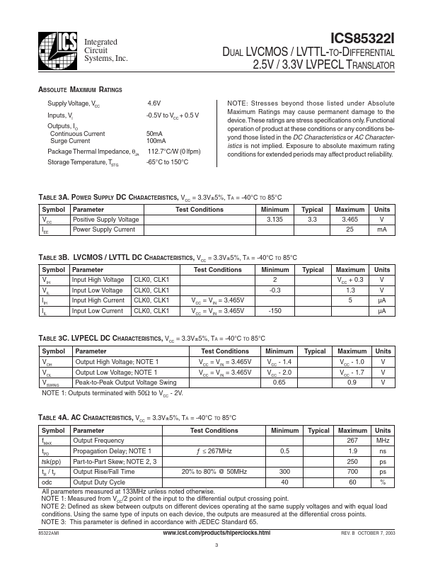
The small outline 8-pin SOIC package makes this device ideal for applications where space, high performance and low power are important. ICS BLOCK DIAGRAM CLK0 Q0 nQ0 Q1 nQ1 PIN ASSIGNMENT Q0 nQ0 Q1 nQ1 1 2 3 4 8 7 6 5 VCC CLK0 CLK1 VEE CLK1 ICS85322I 8-Lead SOIC 3.90mm x 4.92mm x 1.37mm body package M Package Top View 85322AMI 1 REV. B OCTOBER 7, 2003 Integrated Circuit Systems, Inc. ICS85322I DUAL LVCMOS / LVTTL-TO-DIFFERENTIAL 2.5V / 3.3V LVPECL TRANSLATOR Type Output Output Power Input Input Power Pullup PullupDESCRIPTION
Differential output pair.