M1025
M1025 is VCSO BASED CLOCK PLL manufactured by ICST.
DESCRIPTION
The M1025/26 is a VCSO (Voltage Controlled SAW Oscillator) based clock jitter attenuator PLL designed for clock jitter attenuation and frequency translation. The device is ideal for generating the transmit reference clock for optical network systems supporting up to 2.5Gb data rates. It can serve to jitter attenuate a stratum reference clock or a recovered clock in loop timing mode. The M1025/26 module includes a proprietary SAW (surface acoustic wave) delay line as part of the VCSO. This results in a high frequency, high-Q, low phase noise oscillator that assures low intrinsic output jitter.
- Integrated SAW delay line; low phase jitter of < 0.5ps rms, typical (12k Hz to 20MHz)
- Output frequencies of 62.5 to 175 MHz (Specify VCSO output frequency at time of order)
- LVPECL clock output (CML and LVDS options available)
- Reference clock inputs support differential LVDS, LVPECL, as well as single-ended LVCMOS, LVTTL
- Loss of Lock (LOL) output pin; Narrow Bandwidth control input (NBW pin)
- Auto Switch (AUTO pin)
- automatic (non-revertive) reference clock reselection upon clock failure
- Acknowledge pin (REF_ACK pin) indicates the actively selected reference input
- Hitless Switching (HS) options with or without Phase Build-out (PBO) to enable SONET (GR-253) /SDH (G.813) MTIE and TDEV pliance during reselection
- Pin-selectable feedback and reference divider ratios
- Single 3.3V power supply
- Small 9 x 9 mm SMT (surface mount) package
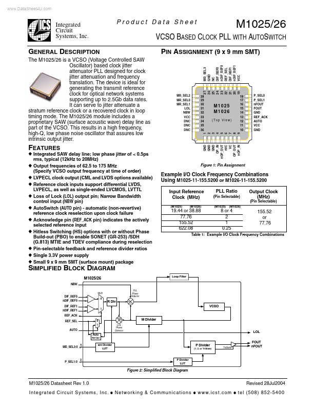
28 29 30 31 32 33 34 35 36
M1025 M1026
(Top View)
18 17 16 15 14 13 12 11 10
P_SEL0 P_SEL1 n FOUT FOUT GND REF_ACK AUTO VCC GND
FEATURES
Figure 1: Pin Assignment
Example I/O Clock Frequency binations Using M1025-11-155.5200 or M1026-11-155.5200
Input Reference Clock (MHz)
(M1025) (M1026)
GND GND GND OP_IN n OP_OUT n VC VC OP_OUT n OP_IN
1 2 3 4 5 6 7 8 9
PLL Ratio
(Pin Selectable)
(M1025) (M1026)
Output Clock (MHz)
(Pin Selectable)
19.44 or 38.88 77.76 155.52 622.08
8 or 4 2 1 0.25
155.52 or 77.76
Table 1:...