Datasheet4U Logo Datasheet4U.com

5PB1108PGG - 1.8V to 3.3V LVCMOS High-Performance Clock Buffer

This page provides the datasheet information for the 5PB1108PGG, a member of the 5PB1102PGG 1.8V to 3.3V LVCMOS High-Performance Clock Buffer family.

Datasheet Summary

Description

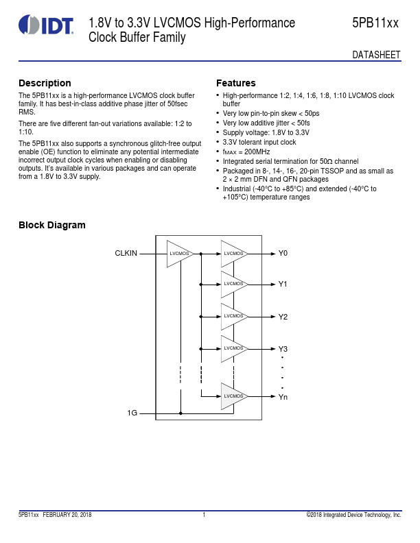
The 5PB11xx is a high-performance LVCMOS clock buffer family.

It has best-in-class additive phase jitter of 50fsec RMS.

There are five different fan-out variations available: 1:2 to 1:10.

Features

  • High-performance 1:2, 1:4, 1:6, 1:8, 1:10 LVCMOS clock buffer.
  • Very low pin-to-pin skew < 50ps.
  • Very low additive jitter < 50fs.
  • Supply voltage: 1.8V to 3.3V.
  • 3.3V tolerant input clock.
  • fMAX = 200MHz.
  • Integrated serial termination for 50 channel.
  • Packaged in 8-, 14-, 16-, 20-pin TSSOP and as small as 2 × 2 mm DFN and QFN packages.
  • Industrial (-40°C to +85°C) and extended (-40°C to +105°C) temperature ranges.

📥 Download Datasheet

Datasheet preview – 5PB1108PGG

Datasheet Details

Part number 5PB1108PGG
Manufacturer IDT
File Size 494.08 KB
Description 1.8V to 3.3V LVCMOS High-Performance Clock Buffer
Datasheet download datasheet 5PB1108PGG Datasheet
Additional preview pages of the 5PB1108PGG datasheet.
Other Datasheets by IDT

Full PDF Text Transcription

Click to expand full text
1.8V to 3.3V LVCMOS High-Performance Clock Buffer Family 5PB11xx DATASHEET Description The 5PB11xx is a high-performance LVCMOS clock buffer family. It has best-in-class additive phase jitter of 50fsec RMS. There are five different fan-out variations available: 1:2 to 1:10. The 5PB11xx also supports a synchronous glitch-free output enable (OE) function to eliminate any potential intermediate incorrect output clock cycles when enabling or disabling outputs. It’s available in various packages and can operate from a 1.8V to 3.3V supply. Features • High-performance 1:2, 1:4, 1:6, 1:8, 1:10 LVCMOS clock buffer • Very low pin-to-pin skew < 50ps • Very low additive jitter < 50fs • Supply voltage: 1.8V to 3.3V • 3.
Published: |