5PB1203
Description
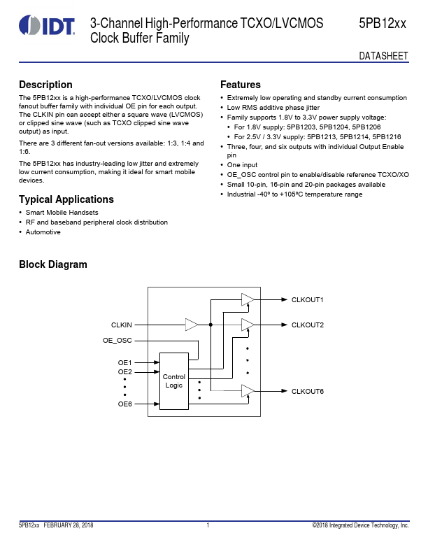
The 5PB12xx is a high-performance TCXO/LVCMOS clock fanout buffer family with individual OE pin for each output.
Key Features
- Extremely low operating and standby current consumption
- Low RMS additive phase jitter
- Family supports 1.8V to 3.3V power supply voltage
- Three, four, and six outputs with individual Output Enable
- OE_OSC control pin to enable/disable reference TCXO/XO
- Small 10-pin, 16-pin and 20-pin packages available
- Industrial -40º to +105ºC temperature range CLKIN OE_OSC
- Same frequency as CLKIN. Clock Output
- Same frequency as CLKIN. Clock Output
- Same frequency as CLKIN. Clock Output
Applications
- Smart Mobile Handsets