87974I
Description
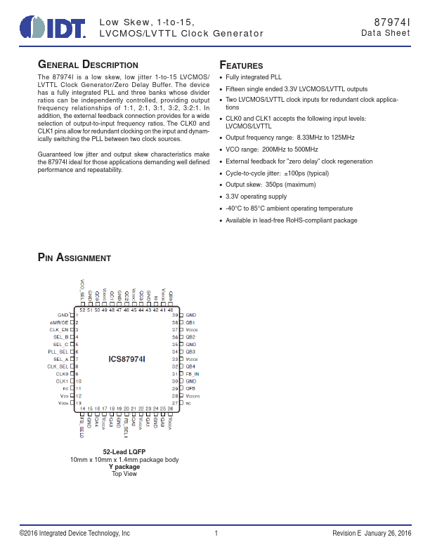
The 87974I is a low skew, low jitter 1-to-15 LVCMOS/ LVTTL Clock Generator/Zero Delay Buffer.
Key Features
- Fully integrated PLL
- Fifteen single ended 3.3V LVCMOS/LVTTL outputs
- Two LVCMOS/LVTTL clock inputs for redundant clock applica- tions
- CLK0 and CLK1 accepts the following input levels: LVCMOS/LVTTL
- Output frequency ran