8T79S308
8T79S308 is 1:8 Universal Differential Fanout Buffer manufactured by IDT.
Description
The 8T79S308 is a fully integrated signal fanout buffer for high-performance, low additive phase noise applications. The main function of the device is the distribution and fanout of high-frequency clocks or low-frequency synchronization signals.
The 8T79S308 is optimized to deliver very low phase noise clocks and precise, low-skew outputs, low device-to-device skew characteristics and fast output rise/fall times help the system design to achieve deterministic clock phase relationship across devices.
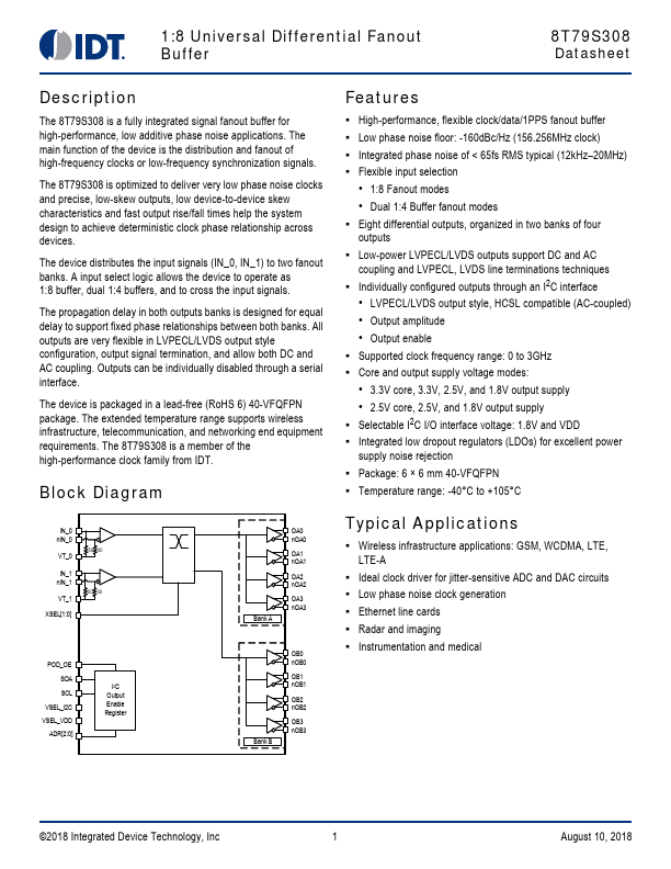
The device distributes the input signals (IN_0, IN_1) to two fanout banks. A input select logic allows the device to operate as 1:8 buffer, dual 1:4 buffers, and to cross the input signals.
The propagation delay in both outputs banks is designed for equal delay to support fixed phase relationships between both banks. All outputs are very flexible in LVPECL/LVDS output style configuration, output signal termination, and allow both DC and AC coupling. Outputs can be individually disabled through a serial interface.
The device is packaged in a lead-free (Ro HS 6) 40-VFQFPN package. The extended temperature range supports wireless infrastructure, telemunication, and networking end equipment requirements. The 8T79S308 is a member of the high-performance clock family from IDT.
Block Diagram
IN_0 n IN_0
VT_0
IN_1 n IN_1
VT_1 XSEL[1:0]
50 50 50 50
Bank A
QA0 n QA0
QA1 n QA1
QA2 n QA2
QA3 n QA3
POD_OE SDA SCL
VSEL_I2C VSEL_VDD
ADR[2:0]
I2C Output Enable Register
Bank B
QB0 n QB0
QB1 n QB1
QB2 n QB2
QB3 n QB3
Features
- High-performance, flexible clock/data/1PPS fanout buffer
- Low phase noise floor: -160d Bc/Hz (156.256MHz clock)
- Integrated phase noise of < 65fs RMS typical (12k Hz- 20MHz)
- Flexible input selection
- 1:8 Fanout modes
- Dual 1:4 Buffer fanout modes
- Eight differential outputs, organized in two banks of four outputs
- Low-power LVPECL/LVDS outputs support DC and AC coupling and LVPECL, LVDS line terminations techniques
- Individually configured outputs...