Datasheet4U Logo Datasheet4U.com

8V19N478 - NG Jitter Attenuator and Clock Synthesizer

Datasheet Summary

Description

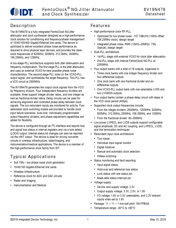
The 8V19N478 is a fully integrated FemtoClock NG jitter attenuator and clock synthesizer designed as a high-performance clock solution for conditioning and frequency/phase management of 10/40/100/400 Gigabit-Ethernet line cards.

Features

  • High-performance clock RF-PLL:.
  • Optimized for low phase noise: -157.7dBc/Hz (1MHz offset; 156.25MHz clock), design target.
  • Integrated phase noise, RMS (12kHz.
  • 20MHz): 73fs (typical), design target.
  • Dual-PLL architecture:.
  • 1st-PLL stage with external VCXO for clock jitter attenuation.
  • 2nd-PLL stage with internal FemtoClock NG PLL at 2500MHz.
  • Four output banks with a total of 18 outputs, organized in:.
  • Three clock banks with one i.

📥 Download Datasheet

Datasheet preview – 8V19N478

Datasheet Details

Part number 8V19N478
Manufacturer IDT
File Size 1.02 MB
Description NG Jitter Attenuator and Clock Synthesizer
Datasheet download datasheet 8V19N478 Datasheet
Additional preview pages of the 8V19N478 datasheet.
Other Datasheets by IDT

Full PDF Text Transcription

Click to expand full text
FemtoClock® NG Jitter Attenuator and Clock Synthesizer 8V19N478 Datasheet Description The 8V19N478 is a fully integrated FemtoClock NG jitter attenuator and clock synthesizer designed as a high-performance clock solution for conditioning and frequency/phase management of 10/40/100/400 Gigabit-Ethernet line cards. The device is optimized to deliver excellent phase noise performance as required to drive physical layer devices, and provides the clean clock frequencies of 625MHz, 500MHz, 312.5MHz, 250MHz, 156.25MHz, and 125MHz. A two-stage PLL architecture supports both jitter attenuation and frequency multiplication. The first stage PLL is the jitter attenuator, and uses an external VCXO for best possible phase noise characteristics.
Published: |