9DB1904B
Overview
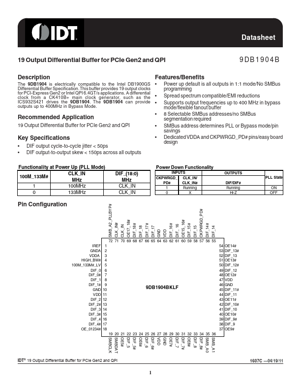
The 9DB1904 is electrically compatible to the Intel DB1900GS Differential Buffer buffer provides 19 output clocks for PCI-Express Gen2 or Intel QPI 6.4GT/s applications. A differential clock from a CK410B+ main clock generator, such as the ICS932S421 drives the 9DB1904.
- Power up default is all outputs in 1:1 mode/No SMBus programming
- Spread spectrum compatible/EMI reductions
- Supports output frequencies up to 400 MHz in bypass mode/flexible fanout buffer
- 8 Selectable SMBus addresses/no SMBus segmentation required
- SMBus address determines PLL or Bypass mode/pin savings
- Dedicated VDDA and CK