9DBL0243 Overview
Key Specifications
Mount Type: Surface Mount
Pins: 24
Operating Voltage: 3.3 V
Max Voltage (typical range): 3.465 V
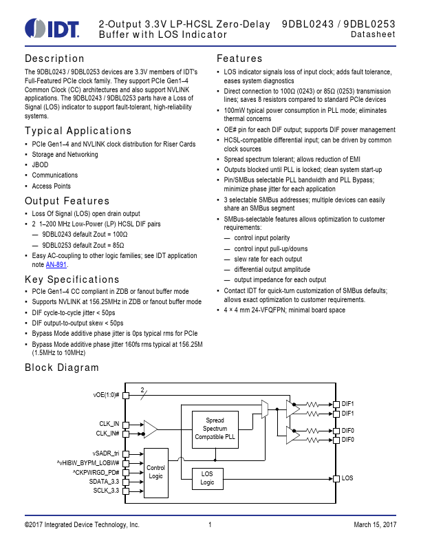
Description
The 9DBL0243 / 9DBL0253 devices are 3.3V members of IDT's Full-Featured PCIe clock family. They support PCIe Gen1–4 Common Clock (CC) architectures and also support NVLINK applications.
Key Features
- 9DBL0243 default Zout = 100Ω