IDT 9DBV0931
The 9DBV0931 is a member of IDT's Full-Featured PCIe family. The device has 9 output enables for clock management, and 3 selectable SMBus addresses.| Part No. | 9DBV0931 |
|---|---|
| Datasheet | 9DBV0931 Download |
| Manufacturer |  IDT |
| Description | 9-output 1.8V HCSL Fanout Buffer |
| Buy | Stock & Price |
DESCRIPTION
Recommended Application PCIe Gen1-3 clock distribution in Storage, Networking, Compute, Consumer OutputFEATURES
● 9 - 1-200MHz Low-Power (LP) HCSL DIF pairs Key Specifications● Additive cycle-to-cycle jitter <5ps
● Output-to-output skew < 60ps
● Additive phase jitter is <100fs rms for PCIe Gen3
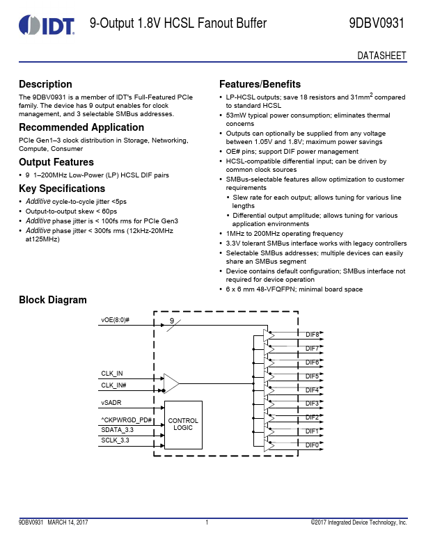
● Additive phase jitter <300fs rms (12kHz-20MHz @125MHz) Block Diagram
FEATURES
/Benefits● LP-HCSL outputs; save 18 resistors and 31mm2 compared to standard HCSL
● 53mW typical power consumption; eliminates thermal concerns
● Outputs can optionally be supplied from any voltage between 1.05V and 1.8V; maximum power savings
● OE# pins; support DIF power management
● HCSL-compatible differential input; can be driven by common clock sources
● SMBus-selectable fea