9FGV0431
Description
The 9FGV0431 is a 4-output very low power clock generator for PCIe Gen 1, 2 and 3 applications. The device has 4 output enables for clock management and supports 2 different spread spectrum levels in addition to spread off.
Remended Application
PCIe Gen1-2-3 Clock Generator
Output Features
- 4
- 0.7V low-power HCSL-patible (LP-HCSL) DIF pairs
- 1
- 1.8V LVCMOS REF output w/Wake-On-Lan
Key Specifications
- DIF cycle-to-cycle jitter <50ps
- DIF output-to-output skew <50ps
- DIF phase jitter is PCIe Gen1-2-3 pliant
- REF phase jitter is < 1.5ps RMS
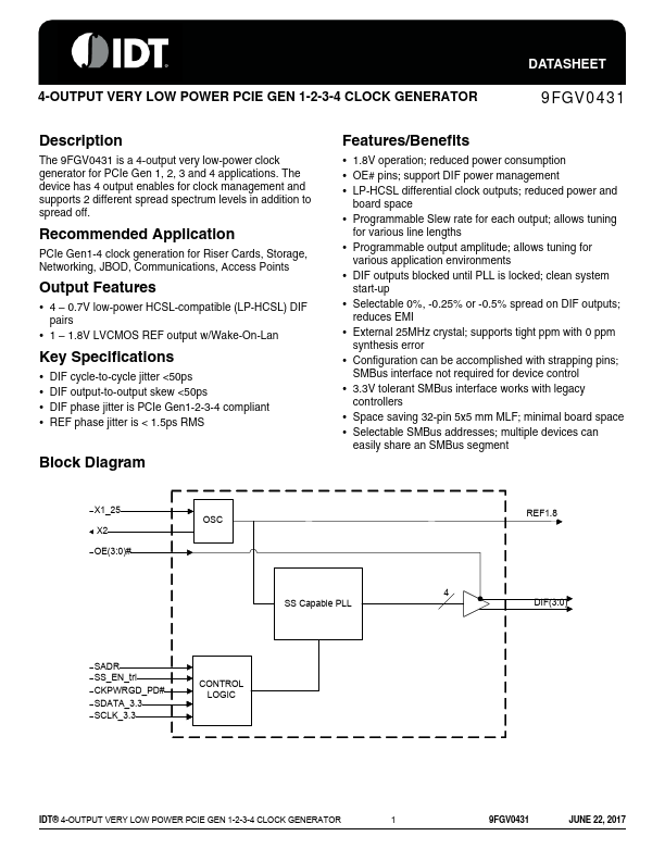
Block Diagram
Features
/Benefits
- 1.8V operation; reduced power consuption
- OE# pins; support DIF power management
- LP-HCSL differential clock outputs; reduced power and board space
- Programmable Slew rate for each output; allows tuning for various line lengths
- Programmable output amplitude; allows tuning for various...


