Datasheet4U Logo Datasheet4U.com

ICS81006I - VCXO-TO-LVCMOS OUTPUTS

General Description

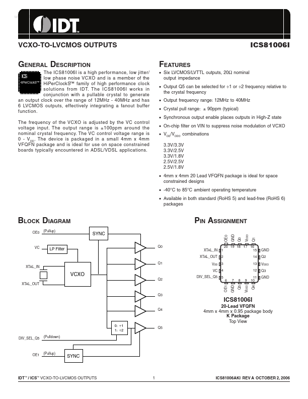
The ICS81006I is a high performance, low jitter/ IC S low phase noise VCXO and is a member of the HiPerClockS™ HiPerClockS™ family of high performance clock solutions from IDT.

Key Features

  • Six LVCMOS/LVTTL outputs, 20Ω nominal output impedance.
  • Output Q5 can be selected for ÷1 or ÷2 frequency relative to the crystal frequency.
  • Output frequency range: 12MHz to 40MHz.
  • Crystal pull range: ± 90ppm (typical).
  • Synchronous output enable places outputs in High-Z state.
  • On-chip filter on VIN to suppress noise modulation of VCXO.
  • VDD/VDDO combinations 3.3V/3.3V 3.3V/2.5V 3.3V/1.8V 2.5V/2.5V 2.5V/1.8V.
  • 4mm x 4mm 20 Lead.

📥 Download Datasheet

Datasheet Details

Part number ICS81006I
Manufacturer IDT
File Size 676.80 KB
Description VCXO-TO-LVCMOS OUTPUTS
Datasheet download datasheet ICS81006I Datasheet

Full PDF Text Transcription (Reference)

The following content is an automatically extracted verbatim text from the original manufacturer datasheet and is provided for reference purposes only.

View original datasheet text
www.DataSheet4U.com VCXO-TO-LVCMOS OUTPUTS ICS81006I GENERAL DESCRIPTION The ICS81006I is a high performance, low jitter/ IC S low phase noise VCXO and is a member of the HiPerClockS™ HiPerClockS™ family of high performance clock solutions from IDT. The ICS81006I works in conjunction with a pullable crystal to generate an output clock over the range of 12MHz - 40MHz and has 6 LVCMOS outputs, effectively integrating a fanout buffer function. The frequency of the VCXO is adjusted by the VC control voltage input. The output range is ±100ppm around the nominal crystal frequency. The VC control voltage range is 0 - V DD . The device is packaged in a small 4mm x 4mm VFQFN package and is ideal for use on space constrained boards typically encountered in ADSL/VDSL applications.