Datasheet4U Logo Datasheet4U.com

ICS843S2807 - CRYSTAL-TOLVPECL/LVDS/LVCMOS CLOCK GENERATOR

General Description

ICS843S2807 is a low phase noise Clock Generator ICS and is a member of the HiperClockS™ family of high HiPerClockS™ performance clock solutions from IDT.

provides five banks of outputs and a reference clock.

The banks can be enabled by using a common output enable pin.

Key Features

  • Five banks of outputs: Bank A: one single-ended (QA0) LVCMOS output at: 133MHz and one (QA1/nQA1) LVPECL output at: 66.67MHz, 100MHz and 125MHz Bank B: two (QB0, QB1) LVCMOS outputs at: 50MHz Bank C: one (QC0/nQC0) differential LVPECL output at: 87.5MHz Bank D: one (QD0/nQD0) differential LVDS output at: 350MHz One single-ended LVCMOS reference clock output at: 25MHz PIN.

📥 Download Datasheet

Datasheet Details

Part number ICS843S2807
Manufacturer IDT
File Size 179.29 KB
Description CRYSTAL-TOLVPECL/LVDS/LVCMOS CLOCK GENERATOR
Datasheet download datasheet ICS843S2807 Datasheet

Full PDF Text Transcription (Reference)

The following content is an automatically extracted verbatim text from the original manufacturer datasheet and is provided for reference purposes only.

View original datasheet text
PRELIMINARY FEMTOCLOCK™ CRYSTAL-TOLVPECL/LVDS/LVCMOS CLOCK GENERATOR
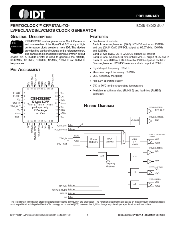
 ICS843S2807 GENERAL DESCRIPTION ICS843S2807 is a low phase noise Clock Generator ICS and is a member of the HiperClockS™ family of high HiPerClockS™ performance clock solutions from IDT. The device provides five banks of outputs and a reference clock. The banks can be enabled by using a common output enable pin. A 25MHz crystal is used to generate the 50MHz, 66.67MHz, 87.5MHz, 100MHz, 125MHz, 133MHz and 350MHz frequencies. FEATURES • Five banks of outputs: Bank A: one single-ended (QA0) LVCMOS output at: 133MHz and one (QA1/nQA1) LVPECL output at: 66.67MHz, 100MHz and 125MHz Bank B: two (QB0, QB1) LVCMOS outputs at: 50MHz Bank C: one (QC0/nQC0) differential LVPECL output at: 87.