Datasheet Summary
56-PIN CK505 W/FULLY INTEGRATED VOLTAGE REGULATOR + INTEGRATED SERIES RESISTOR
Remended Application:
CK505 pliant clock with fully integrated voltage regulator and Internal series resistor on differential outputs, PCIe Gen 1 pliant
Key Specifications:
- -
- - CPU outputs cycle-cycle jitter < 85ps SRC output cycle-cycle jitter < 125ps PCI outputs cycle-cycle jitter < 250ps +/- 100ppm frequency accuracy on CPU & SRC clocks
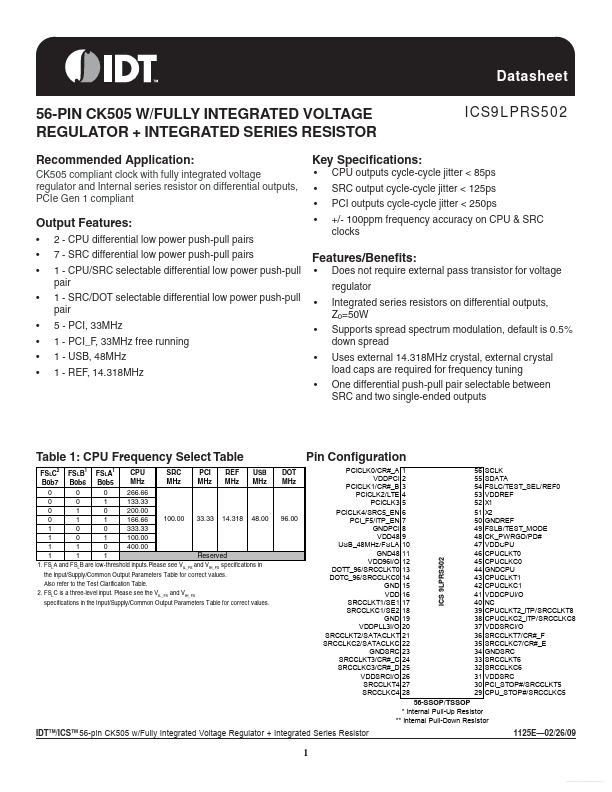
Output Features
:
- -
- -
- -
- - 2
- CPU differential low power push-pull pairs 7
- SRC differential low power push-pull pairs 1
- CPU/SRC selectable differential low power push-pull pair 1
- SRC/DOT selectable differential low power...