Datasheet4U Logo Datasheet4U.com

IDT5V928 - 8 OUTPUT CLOCK GENERATOR

Datasheet Summary

Description

APPLICATIONS: Gigabit ethernet Router Network switches SAN Instrumentation Fibre channel FUNCTIONAL BLOCK DIAGRAM OE VCO DIVIDE 1/N Q0 REF PH AS E DETEC TO R CH ARGE PU M P LO OP FILTER VC O Q1 Q2 0 Q3 1 Q4 Q5 X2 CRY STAL OSCILLATO R X

Features

  • 3V to 3.6V operating voltage 50MHz to 160MHz output frequency range Input from fundamental crystal oscillator or external source Internal PLL feedback (loading feedback output relative to other outputs, adjusts propagation delay between REF inputs and outputs) Select inputs (S[1:0]) for FB divide selection (multiply ratio of 2, 3, 4, 4.25, 5, 6, 6.25, and 8) Low jitter PLL bypass for testing and power-down control.

📥 Download Datasheet

Datasheet preview – IDT5V928

Datasheet Details

Part number IDT5V928
Manufacturer IDT
File Size 48.36 KB
Description 8 OUTPUT CLOCK GENERATOR
Datasheet download datasheet IDT5V928 Datasheet
Additional preview pages of the IDT5V928 datasheet.
Other Datasheets by IDT

Full PDF Text Transcription

Click to expand full text
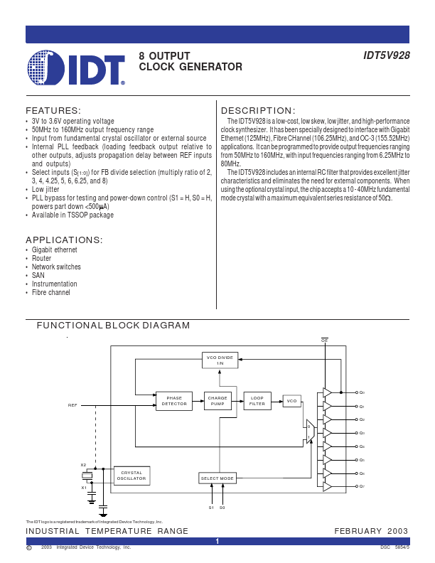
IDT5V928 8 OUTPUT CLOCK GENERATOR INDUSTRIAL TEMPERATURE RANGE 8 OUTPUT CLOCK GENERATOR IDT5V928 FEATURES: • • • • • • • • 3V to 3.6V operating voltage 50MHz to 160MHz output frequency range Input from fundamental crystal oscillator or external source Internal PLL feedback (loading feedback output relative to other outputs, adjusts propagation delay between REF inputs and outputs) Select inputs (S[1:0]) for FB divide selection (multiply ratio of 2, 3, 4, 4.25, 5, 6, 6.25, and 8) Low jitter PLL bypass for testing and power-down control (S1 = H, S0 = H, powers part down <500µ A) Available in TSSOP package The IDT5V928 is a low-cost, low skew, low jitter, and high-performance clock synthesizer.
Published: |