IDT72T1865
Key Features
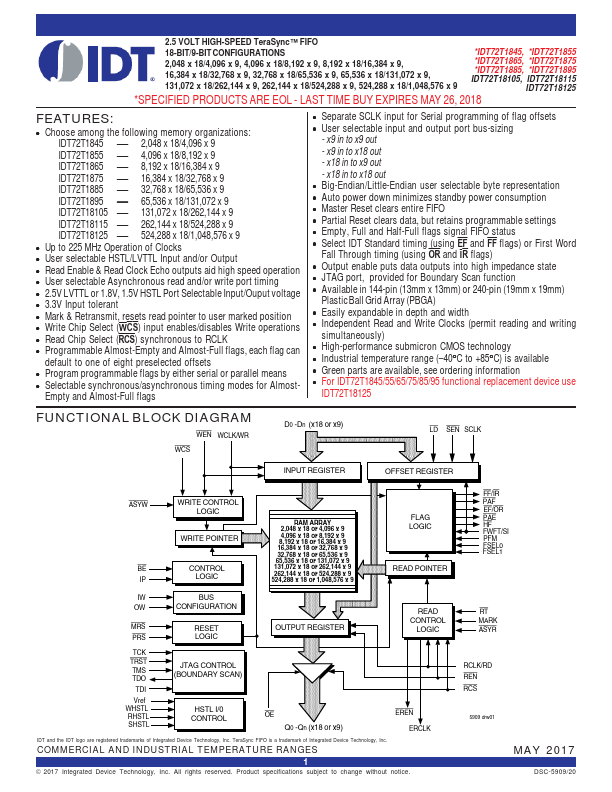
- Choose among the following memory organizations: IDT72T1845 2,048 x 18/4,096 x 9 IDT72T1855 4,096 x 18/8,192 x 9 IDT72T1865 8,192 x 18/16,384 x 9 IDT72T1875 16,384 x 18/32,768 x 9 IDT72T1885 32,768 x 18/65,536 x 9 IDT72T1895 65,536 x 18/131,072 x 9 IDT72T18105 131,072 x 18/262,144 x 9 IDT72T18115 262,144 x 18/524,288 x 9 IDT72T18125 524,288 x 18/1,048,576 x 9 Up to 225 MHz Operation of Clocks User selectable HSTL/LVTTL Input and/or Output Read Enable & Read Clock Echo outputs aid high speed operation User selectable Asynchronous read and/or write port timing 2.5V LVTTL or 1.8V, 1.5V HSTL Port Selectable Input/Ouput voltage 3.3V Input tolerant Mark & Retransmit, resets read pointer to user marked position Write Chip Select (WCS) input enables/disables Write operations Read Chip Select (RCS) synchronous to RCLK Programmable Almost-Empty and Almost-Full flags, each flag can default to one of eight preselected offsets Program programmable flags by either serial or parallel means Selectable synchronous/asynchronous timing modes for Almost- * * * * * * * * * * * * * *
- Empty and Almost-Full flags Separate SCLK input for Serial programming of flag offsets User selectable input and output port bus-sizing - x9 in to x9 out - x9 in to x18 out - x18 in to x9 out - x18 in to x18 out Big-Endian/Little-Endian user selectable byte representation Auto power down minimizes standby power consumption Master Reset clears entire FIFO Partial Reset cle