IDT74SSTVF16859
Overview
- 1:2 register buffer Meets or exceeds JEDEC standard SSTVF16859 2.3V to 2.7V Operation for PC1600, PC2100, and PC2700 2.5V to 2.7V Operation for PC3200 SSTL_2 Class I style data inputs/outputs Differential CLK input RESET control compatible with LVCMOS levels Latch-up performance exceeds 100mA ESD >2000V per MIL-STD-883, Method 3015; >200V using machine model (C = 200pF, R = 0)
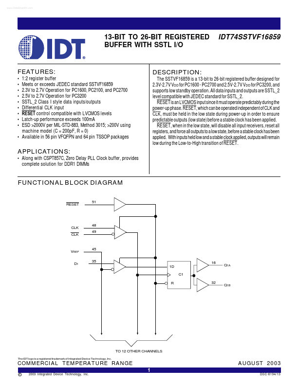
- Available in 56 pin VFQFPN and 64 pin TSSOP packages The SSTVF16859 is a 13-bit to 26-bit registered buffer designed for 2.3V-2.7V VDD for PC1600 - PC2700 and 2.5V-2.7V VDD for PC3200, and supports low standby operation. All data inputs and outputs are SSTL_2 level compatible with JEDEC standard for SSTL_2. RESET is an LVCMOS input since it must operate predictably during the power-up phase. RESET, which can be operated independent of CLK and CLK, must be held in the low state during power-up in order to ensure predictable outputs (low state) before a stable clock has been applied. RESET, when in the low state, will disable all input receivers, reset all registers, and force all outputs to a low state, before a stable clock has been applied. With inputs held low and a stable clock applied, outputs will remain low during the Low-to-High transition of RESET.