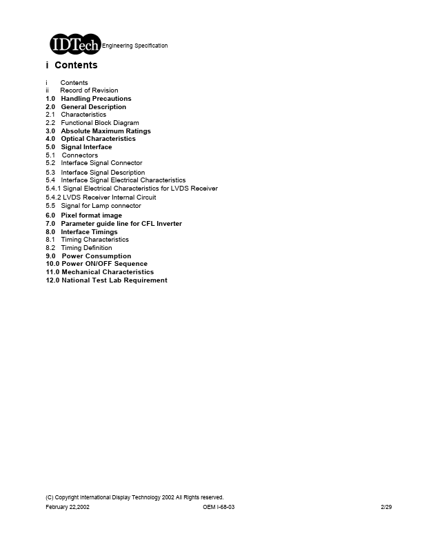
GENERAL DESCRIPTION
2.1 Characteristics 2.2 Functional Block Diagram 3.0 ABSOLUTE MAXIMUM RATINGS
4.0 Optical Characteristics 5.0 Signal Interface 5.1 Connectors 5.2 Interface Signal Connector 5.3 Interface Signal DESCRIPTION
5.4 Interface Signal ELECTRICAL CHARACTERISTICS
5.4.1 Signal ELECTRICAL CHARACTERISTICS
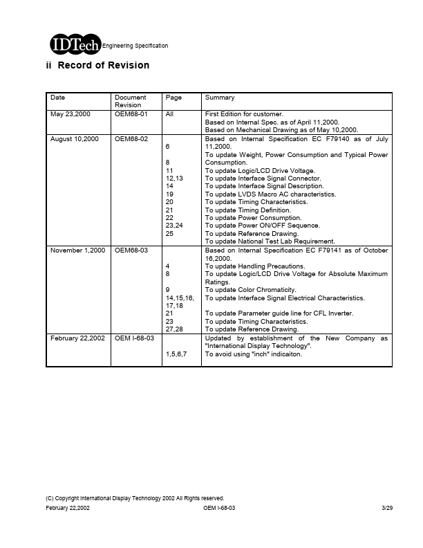
for LVDS Receiver 5.4.2 LVDS Receiver Internal Circuit 5.5 Signal for Lamp connector 6.0 Pixel format image 7.0 Parameter guide line for CFL Inverter 8.0 Interface Timings 8.1 Timing Characteristics 8.2 Timing Definition 9.0 Power Consumption 10.0 Power ON/OFF Sequence 11.0 Mechanical Characteristics 12.0 National Test Lab Requirement (C) Copyright International Display Technology 2002 All Rights reserved. February 22,2002 OEM I-68-03 2/29 Engineering Specification ii Record of Revision Date May 23,2000 Document Revision OEM68-01 August 10,2000 OEM68-02 November 1,2000 OEM68-03 February 22,2002 OEM I-68-03 Page All 6 8 11 12,13 14 19 20 21 22 23,24 25 4 8 9 14,15,16, 17,18 21 23 27,28 1,5,6,7 Summary First Edition for customer. IDTech