GENERAL DESCRIPTION
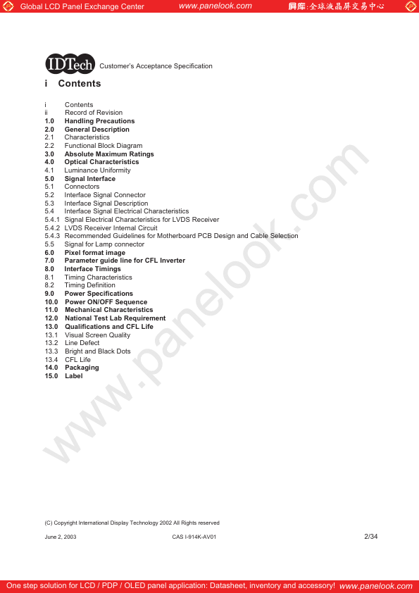
2.1 Characteristics 2.2 Functional Block Diagram 3.0 ABSOLUTE MAXIMUM RATINGS
4.0 Optical Characteristics 4.1 Luminance Uniformity 5.0 Signal Interface 5.1 Connectors 5.2 Interface Signal Connector 5.3 Interface Signal DESCRIPTION
5.4 Interface Signal ELECTRICAL CHARACTERISTICS
5.4.1 Signal ELECTRICAL CHARACTERISTICS
for LVDS Receiver 5.4.2 LVDS Receiver Internal Circuit 5.4.3 Recommended Guidelines for Motherboard PCB Design and Cable Selection 5.5 Signal for Lamp connector 6.0 Pixel format image 7.0 Parameter guide line for CFL Inverter 8.0 Interface Timings 8.1 Timing Characteristics 8.2 Timing Definition 9.0 Power Specifications 10.0 Power ON/OFF Sequence 11.0 Mechanical Characteristics 12.0 National Test Lab Requirement 13.0 Qualifications and CFL Life 13.1 Visual Screen Quality 13.2 Line Defect 13.3 Bright and Black Dots 13.4 CFL Life 14.0 Packaging 15.0 Label (C) Copyright International Display Technology 2002 All Rights reserved June 2, 2003 CAS I-914K-AV01 2/34 One step solution for LCD / PDP / OLED panel application: Datasheet, inventory and accessory! IDtech